L6206 Просмотр технического описания (PDF) - STMicroelectronics
Номер в каталоге
Компоненты Описание
производитель
L6206 Datasheet PDF : 23 Pages
| |||
L6206
CIRCUIT DESCRIPTION
POWER STAGES and CHARGE PUMP
The L6206 integrates two independent Power MOS
Full Bridges. Each Power MOS has an Rd-
son=0.3ohm (typical value @ 25°C), with intrinsic
fast freewheeling diode. Cross conduction protection
is achieved using a dead time (td = 1µs typical) be-
tween the switch off and switch on of two Power MOS
in one leg of a bridge.
Using N Channel Power MOS for the upper transis-
tors in the bridge requires a gate drive voltage above
the power supply voltage. The Bootstrapped (Vboot)
supply is obtained through an internal Oscillator and
few external components to realize a charge pump
circuit as shown in Figure 3. The oscillator output
(VCP) is a square wave at 600kHz (typical) with 10V
amplitude. Recommended values/part numbers for
the charge pump circuit are shown in Table1.
Table 1. Charge Pump External Components
Values
CBOOT
CP
RP
D1
220nF
10nF
100Ω
1N4148
D2
1N4148
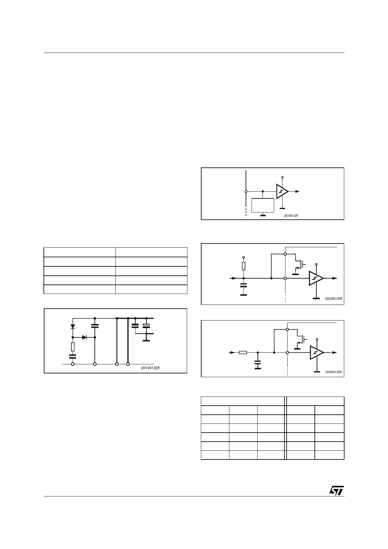
Figure 3. Charge Pump Circuit
VS
D1
D2
CBOOT
RP
CP
VCP VBOOT
VSA VSB D01IN1328
LOGIC INPUTS
Pins IN1A, IN2A, IN1B, IN2B, ENA and ENB are TTL/
CMOS and uC compatible logic inputs. The internal
structure is shown in Fig. 4. Typical value for turn-on
and turn-off thresholds are respectively Vthon=1.8V
and Vthoff = 1.3V.
Pins ENA and ENB are commonly used to implement
Overcurrent and Thermal protection by connecting
them respectively to the outputs OCDA and OCDB,
which are open-drain outputs. If that type of connec-
tion is chosen, some care needs to be taken in driving
these pins. Two configurations are shown in Fig. 5
and Fig. 6. If driven by an open drain (collector) struc-
ture, a pull-up resistor REN and a capacitor CEN are
connected as shown in Fig. 5. If the driver is a stan-
dard Push-Pull structure the resistor REN and the ca-
pacitor CEN are connected as shown in Fig. 6. The
resistor REN should be chosen in the range from
2.2kΩ to 180KΩ. Recommended values for REN and
CEN are respectively 100KΩ and 5.6nF. More infor-
mation on selecting the values is found in the Over-
current Protection section.
Figure 4. Logic Inputs Internal Structure
5V
ESD
PROTECTION
D01IN1329
Figure 5. ENA and ENB Pins Open Collector
Driving
5V
OCDA or OCDB
5V
REN
OPEN
COLLECTOR
OUTPUT
CEN ENA or ENB
D02IN1355
Figure 6. ENA and ENB Pins Push-Pull Driving
OCDA or OCDB
5V
PUSH-PULL
OUTPUT
REN
CEN
ENA or ENB
D02IN1356
TRUTH TABLE
INPUTS
EN
IN1
IN2
OUTPUTS
OUT1 OUT2
L
X
X
High Z High Z
H
L
L
GND
GND
H
H
L
Vs
GND
H
L
H
GND
Vs
H
H
H
Vs
Vs
X
= Don't care
High Z = High Impedance Output
8/23
Share Link: 