MAX189AEPA(2012) Просмотр технического описания (PDF) - Maxim Integrated
Номер в каталоге
Компоненты Описание
производитель
MAX189AEPA Datasheet PDF : 18 Pages
| |||
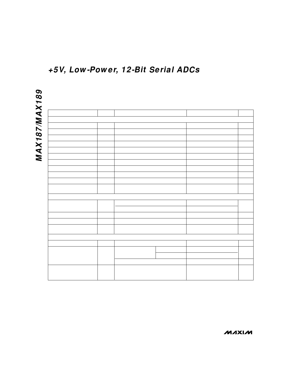
MAX187/ MAX189
+5V, Low-Power, 12-Bit Serial ADCs
ELECTRICAL CHARACTERISTICS (continued)
(VDD = +5V ±5%; VGND = 0V; unipolar input mode; 75ksps, fCLK = 4.0MHz, external clock (50% duty cycle); MAX187—internal refer-
ence: VREF = 4.096V, 4.7µF capacitor at REF pin, or MAX189—external reference: VREF = 4.096V applied to REF pin, 4.7µF capacitor
at REF pin; TA = TMIN to TMAX; unless otherwise noted.)
PARAMETER
DIGITAL OUTPUT (DOUT)
Output Voltage Low
Output Voltage High
Three-State Leakage Current
Three-State Output Capacitance
POWER REQUIREMENTS
Supply Voltage
Supply Current
Power-Supply Rejection
SYMBOL
CONDITIONS
VOL
VOH
IL
COUT
ISINK = 5mA
ISINK = 16mA
ISOURCE = 1mA
VCS = 5V
VCS = 5V (Note 4)
VDD
Operating mode
IDD
MAX187
MAX189
Power-down mode
PSR
VDD = +5V Q5%; external reference,
4.096V; full-scale input (Note 6)
MIN TYP MAX UNITS
0.4
V
0.3
4
V
Q10
FA
15
pF
4.75
5.25
V
1.5
2.5
mA
1.0
2.0
2
10
FA
Q0.06 Q0.5
mV
TIMING CHARACTERISTICS
(VDD = +5V ±5%, TA = TMIN to TMAX; unless otherwise noted.)
PARAMETER
Track/Hold Acquisition Time
SCLK Fall to Output Data Valid
CS Fall to Output Enable
CS Rise to Output Disable
SCLK Clock Frequency
SCLK Pulse Width High
SCLK Pulse Width Low
SCLK Low to CS Fall Setup Time
CS Pulse Width
SYMBOL
CONDITIONS
tACQ
tDQ
CS = high (Note7)
CLOAD = 100pF
MAX18_ _C/E
MAX18_ _M
tDV
tTR
tSCLK
tCH
tCL
tCSO
tCS
CLOAD = 100pF
CLOAD = 100pF
MIN TYP MAX UNITS
1.5
µs
20
150
ns
20
200
100
ns
100
ns
5
MHz
100
ns
100
ns
50
ns
500
ns
Note 1: Tested at VDD = +5V.
Note 2: Relative accuracy is the deviation of the analog value at any code from its theoretical value after the full-scale range has
been calibrated.
Note 3: MAX187—internal reference, offset nulled; MAX189–external +4.096V reference, offset nulled. Excludes reference errors.
Note 4: Guaranteed by design. Not subject to production testing.
Note 5: External load should not change during conversion for specified ADC accuracy.
Note 6: DC test, measured at 4.75V and 5.25V only.
Note 7: To guarantee acquisition time, tACQ is the maximum time the device takes to acquire the signal, and is also the minimum-
time needed for the signal to be acquired.
Maxim Integrated
4
Share Link: 