SXA-289 Просмотр технического описания (PDF) - Stanford Microdevices
Номер в каталоге
Компоненты Описание
производитель
SXA-289 Datasheet PDF : 6 Pages
| |||
Absolute Maximum Ratings
Parameter
Absolute Maximum
Device Voltage
6V
Device Current
200mA
Power Dissipation
1500mW
RF Input Power
100mW
Junction Temperature
+150C
Operating Temperature
-40C to +85C
Storage Temperature
-65C to +150C
Caution: ESD sensitive
Appropriate precautions in handling, packaging and
testing devices must be observed.
SXA-289 5-2000 MHz Power Amplifier
Part Number Ordering Information
Part Number Devices Per Reel Reel Size
SXA-289
1000
7"
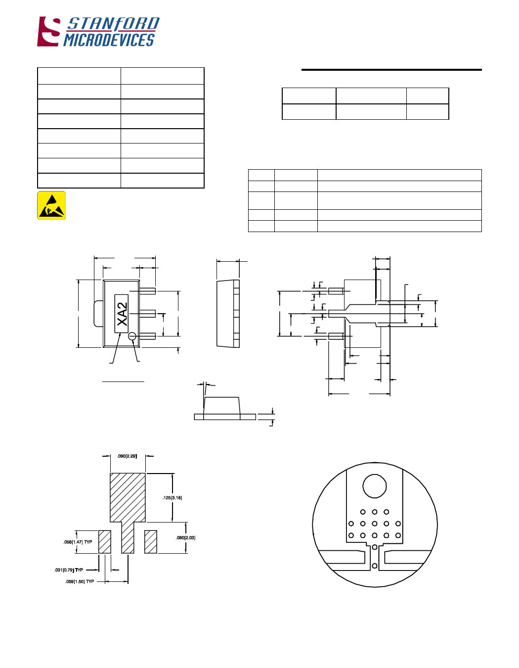
Pin #
1
2
3
4
Part Symbolization
The part will be symbolized with a “XA2”
designator on the top surface of the package.
Pin Description
Function
Description
Base
Base Pin
GND & Emitter
Connection to ground. Use via holes to reduce lead inductance.
Place vias as close to ground leads as possible.
Collector Collector Pin
GND & Emitter Same as Pin 2
.161±.006
.096±.006
.041±.006
.177±.004
.118±.003
.059±.003
.030±.004
MARKING AREA
DOT DENOTES
PIN 1
TOP VIEW
Package Dimensions
.059±.004
.008
.038±.002
.036±.002
.016REF
.010
.118REF
.019
.059
+.003
-.002
.016+-..000023
5°+-43°°
.041REF
.105±.002
.117±.002
.024±.004
.161 REF
.048±.002
.010±.002 TYP(2X)
.068±.004
.034
PCB Pad Layout
.015
+.002
-.001
TYP(4X)
Recommended via and mounting hole pattern
(For RF Ground and Thermal considerations)
DIMENSIONS ARE IN INCHES [MM]
Use multiple plated-through vias holes located close to the package pins to ensure a good RF ground connection to a
continuous groundplane on the backside of the board.
522 Almanor Ave., Sunnyvale, CA 94085
Phone: (800) SMI-MMIC
6
http://www.stanfordmicro.com
EDS-100622 Rev E
Share Link: 