MC145705 Просмотр технического описания (PDF) - Motorola => Freescale
Номер в каталоге
Компоненты Описание
производитель
MC145705 Datasheet PDF : 12 Pages
| |||
PIN DESCRIPTIONS
VCC
Digital Power Supply
This digital supply pin is connected to the logic power sup-
ply. This pin should have a 0.33 µF capacitor to ground.
GND
Ground
Ground return pin is typically connected to the signal
ground pin of the EIA–232–D connector (Pin 7) as well as to
the logic power supply ground.
VDD
Positive Power Supply
This is the positive output of the on–chip voltage doubler
and the positive power supply input of the driver/receiver
sections of the device. This pin requires an external storage
capacitor to filter the 50% duty cycle voltage generated by
the charge pump.
VSS
Negative Power Supply
This is the negative output of the on–chip voltage doubler/
inverter and the negative power supply input of the driver/
receiver sections of the device. This pin requires an external
storage capacitor to filter the 50% duty cycle voltage gener-
ated by the charge pump.
TxEN
Output Enable
This is the driver output enable pin. When this pin is in
logic low level, the condition of the driver outputs (Tx1 – Tx3)
are in keep OFF (mark) state.
STB
Standby
The device enters the standby mode while this pin is con-
nected to the logic high level. During the standby mode,
driver and receiver output pins become high impedance
state. In this condition, supply current ICC is below 10 µA
(Typ) and can be operated with low current consumption.
C2+, C2–, C1+, C1–
Voltage Doubler and Inverter
These are the connections to the internal voltage doubler
and inverter, which generate the VDD and VSS voltages.
Rx1, Rx2 (Rx3)
Receive Data Input
These are the EIA–232–E receive signal inputs. A voltage
between + 3 and + 25 V is decoded as a space, and causes
the corresponding DO pin to swing to ground (0 V). A voltage
between – 3 and – 25 V is decoded as a mark, and causes
the DO pin to swing up to VCC.
DO1, DO2 (DO3)
Data Output
These are the receiver digital output pins, which swing
from VCC to GND. Each output pin is capable of driving one
LSTTL input load.
Output level of these pins is high impedance while in
standby mode.
DI1, DI2 (DI3)
Data Input
These are the high impedance digital input pins to the
drivers. Input voltage levels on these pins must be between
VCC and GND.
The level of these input pins are TTL/CMOS compatible.
Tx1, Tx2 (Tx3)
Transmit Data Output
These are the EIA–232–E transmit signal output pins,
which swing toward VDD and VSS. A logic 1 at a DI input
causes the corresponding Tx output to swing toward VSS.
The actual levels and slew rate achieved will depend on the
output loading (RL/CL).
The minimum output impedance is 300 Ω when turned off.
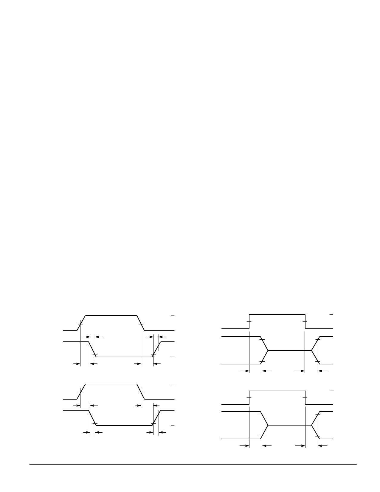
SWITCHING CHARACTERISTICS
DRIVER
DI1 – DI3
(INPUT)
50%
Tx1 – Tx3
(OUTPUT)
tf
90%
10%
tPHL
tPLH
RECEIVER
Rx1 – Rx3
(INPUT)
DO1 – DO3
(OUTPUT)
50%
tPHL
90%
10%
tf
+3V
0V
tr
VOH
VOL
+3V
0V
tPLH
VOH
VOL
tr
DRIVER
STB (INPUT)
Tx1 – Rx3
(OUTPUT)
tDAZ
RECEIVER
STB (INPUT)
DO1 – DO3
(OUTPUT)
tRAZ
+ 1.5 V
+5V
–5V
+ 1.5 V
90%
10%
HIGH Z
tDZA
+5V
+ 1.5 V
0V
+ 5 V VOH
–5V
VOL
HIGH Z
+5V
+ 1.5 V
0V
90% VOH
10%
VOL
tRZA
MC145705•MC145706•MC145707
6
MOTOROLA
Share Link: 