PCF5077T Просмотр технического описания (PDF) - Philips Electronics
Номер в каталоге
Компоненты Описание
производитель
PCF5077T Datasheet PDF : 24 Pages
| |||
Philips Semiconductors
Power amplifier controller for GSM and
PCN systems
Preliminary specification
PCF5077T
Serial bus programming
A simple 3-wire unidirectional serial bus is used to program
the circuit. The 3 wires are DATA, CLK and STROBE.
The data sent to the device is loaded in bursts framed by
STROBE. Programming clock edges and their appropriate
data bits are ignored until STROBE goes active LOW.
The last four address bits are decoded on the active
STROBE edge. This produces an internal load pulse to
store the data in one of the addressed registers. To avoid
erroneous circuit operation, the STROBE pulse is not
allowed during internal data reads by the rest of the circuit.
This condition is guaranteed by respecting a minimum
STROBE pulse width after data transfer.
Only the last 16 bits serially clocked into the device are
retained within the programming register. Additional
leading bits are ignored, and no check is made on the
number of clock pulses. The fully static CMOS design uses
virtually no current when the bus is inactive. The bus is
also programmable during power-down.
Data format
Data is entered with the most significant bit (MSB) first.
The leading 10 bits p15 to p6 are the data field, the
following bits p5 and p4 form the subaddress, while the
last 4 bits p3 to p0 are the device address field.
The PCF5077T uses only one of the available addresses.
The format is given in Table 2.
The correspondence between data and address fields is
given in Table 3 and the description in Table 4.
All three registers in Table 3 are set to 00H during reset.
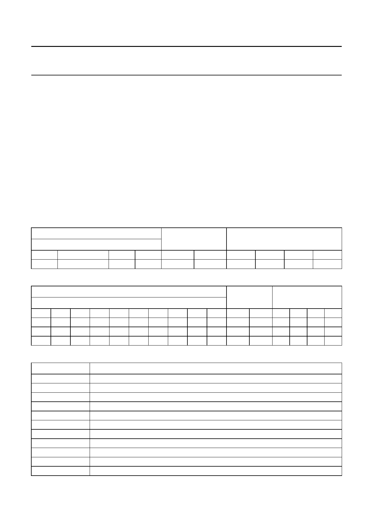
Table 2 Programming register format
DATA BITS
MSB
p15
data9
p14 to p8
data8 to data2
p7
data1
LSB
p6
data0
SUBADDRESS
p5
Sadd1
p4
Sadd0
DEVICE ADDRESS
p3
add3
p2
add2
p1
add1
p0
add0
Table 3 Register bit allocation
MSB
DATA FIELD (D9 TO D0)
SUBADDRESS DEVICE ADDRESS
LSB
p15 p14 p13 p12 p11 p10 p9 p8 p7 p6 p5
p4 p3 p2 p1 p0
Vk5 Vk4 Vk3 Vk2 Vk1 Vk0 Lim1 Lim0 DC Test 0
0
1010
Vh5 Vh4 Vh3 Vh2 Vh1 Vh0 DVh1 DVh0 DR1 DR0 0
1
1010
PL7 PL6 PL5 PL4 PL3 PL2 PL1 PL0 DF1 DF0 1
1
1010
Table 4 Description of bits used in Table 3
BITS
Vk5 to Vk0
Vh5 to Vh0
PL7 to PL0
Lim1 and Lim0
DC
Test
DVh1 and DVh0
DR1
DR0
DF1
DF0
DESCRIPTION
6 bits to control the kick voltage in 64 steps
6 bits to control the home position voltage in 64 steps
8 bits to control the power level in 256 steps
2 bits to control the limiter voltage (see Table 5)
direct control with ramping function (control loop is switched off when DC = 1)
test mode (Test = 1); must always be set to logic 0 in application
2 bits to set the temperature coefficient of VHOME (see Table 6)
gain factor of OP1
gain factor for slope generator output
enable of the 3-state output on pin DF (for DF1 = 0, pin DF is in 3-state mode)
data output on pin DF
1997 Nov 19
8
Share Link: 