PCF5077T Просмотр технического описания (PDF) - Philips Electronics
Номер в каталоге
Компоненты Описание
производитель
PCF5077T Datasheet PDF : 24 Pages
| |||
Philips Semiconductors
Power amplifier controller for GSM and
PCN systems
Preliminary specification
PCF5077T
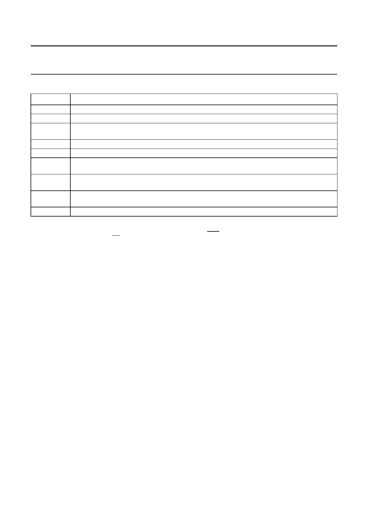
Table 1 Definition of some voltages used in Figs 1 and 3
SYMBOL
Vref
VD1
VPL
VVS
VBVS
VKICK
VHOME
VQRS
VRFIN
DESCRIPTION
reference voltage, typically 1.25 V
voltage over the sensor diode D1
voltage determining the power level; it is generated in the Switched Capacitor (SC)-adder block if
switch DACA is closed (i.e. if the signal DACA is HIGH)
voltage at pin VS when RF is rectified by the sensor diode D1
amplified voltage from pin VS
voltage determining the kick level; it is generated in the SC-adder block if switch KICKA is closed (i.e.
if the signal KICKA is HIGH)
voltage determining the home position voltage; if HPA signal is active, the output of DAC6 plus
temperature compensation is amplified and appears at the output of OP4 (pin VINT(O))
low voltage at the output of the SC-adder block which causes a ramp-down with a shortened tail if
switch QRSA is closed (i.e. if the signal QRSA is HIGH)
input signal to the power amplifier
Ramp generation (see Fig.3)
The circuit is activated with the PD signal going HIGH
before time mask AS and deactivated after ramping down,
e.g. at time GS to HS. For this usual ‘power-down burst
mode’ application in GSM/PCN mobile stations, the RF
input power at the power module must be activated
between time AS and BS (when the home position at
VINT(O) has already reached its stable value) and
deactivated between time GS and HS. This is necessary
for many types of power modules to meet the −70 dB
margin.
A ramp-up is started by a rising edge of the TRIG signal.
The TRIG signal and all other internal signals are delayed
by two clock periods (2Tcy) with respect to the signal at
pin TRIG.
The timing diagram shows a possible relationship between
the chip timing (time B to G) relative to the GSM-mask
(AS to HS). However, the user is free to choose the rising
and falling edge of TRIG independently so that the mask is
not violated.
DESCRIPTION OF THE SIGNALS STARTING AT A STABLE HOME
POSITION OF VINT(O) AT TIME B − 2Tcy
The integrator output voltage is regulated to the value
defined in the VHOME register. The output of the slope
generator is connected to the negative input VINT(N) of
operational amplifier OP4 (VKICK is defined by
bits Vk5 to Vk0 in the VKICK register). Two clock periods
after a rising edge on pin TRIG, the integrator start
condition circuitry is turned off and OP4 is switched into an
integrator configuration (time B). The HPA switches will
open (HPA + DC is either HPA switch or DC bit).
Switch HPA is closed when there is no home position.
Due to the negative differential input voltage VKICK, the
integrator output will start to rise. After 18Tcy (time C) the
output of DAC8 is connected to the SC-adder and slope
generator block. The input of the 8-bit DAC comes from
bits PL7 to PL0 in the power level register. The slope
generator will generate a smooth curve between the
former and the new output value of the SC-adder block.
The power amplifier is ramped-up via the integrator in
approximately 22Tcy.
This condition is stable as long as TRIG remains HIGH.
Two clock periods after a falling edge at TRIG the
ramp-down is started (time E). The SC-adder output
voltage will change to VQRS (−100 mV), because DACA
becomes inactive and QRSA active. This causes a
ramp-down with a shortened tail. The slope generator
again generates a smooth curve between the new
SC-adder output voltage and the old SC-adder output
voltage.
The slope generator must have reached its final value at
38Tcy after the recognized falling edge of TRIG because
the HPA signal is activated again and by that turning the
integrator into its ‘home position’ (time G). The integrator
output voltage will be regulated once more to the value
defined in the VHOME register.
1997 Nov 19
6
Share Link: 