PCF5077T Просмотр технического описания (PDF) - Philips Electronics
Номер в каталоге
Компоненты Описание
производитель
PCF5077T Datasheet PDF : 24 Pages
| |||
Philips Semiconductors
Power amplifier controller for GSM and
PCN systems
Preliminary specification
PCF5077T
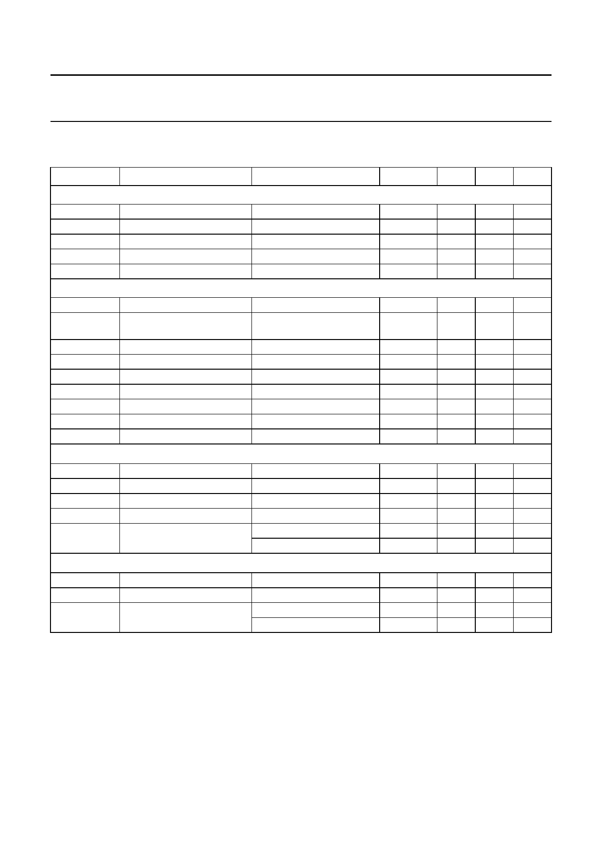
OPERATING CHARACTERISTICS
VDDA1, VDDA2 and VDDD = VDD = 2.7 to 6.0 V; VDDD = VDDA1 ≤ VDDA2; Tamb = −40 to +85 °C; unless otherwise specified.
SYMBOL
PARAMETER
CONDITIONS
MIN.
TYP. MAX. UNIT
Operational amplifier (OP1)
VDDA1
GB
Gmin
Gmax
Voffset
analog supply voltage 1
gain bandwidth product
minimum gain
maximum gain
offset voltage
VDDA1 = 3.0 V
DR1 = 0
DR1 = 1
no load at output
Operational amplifier (OP4)
VDDA2
GB
analog supply voltage 2
gain bandwidth product
CL = 120 pF; VDDA2 = 5 V;
note 2
PSRR
SRpos
SRneg
Voffset
Vo(min)
Vo(max)
Io
power supply rejection ratio
positive slew rate
negative slew rate
voltage offset
minimum output voltage
maximum output voltage
output current
VDDA2 = 5 V, at 217 Hz
VDDA2 = 5 V; note 4
VDDA2 = 5 V; note 4
no load at output
note 5
Programmability and accuracy of VPL (DAC8) at VINT(O)
INL
integral non-linearity
DNL
differential non-linearity
Vo(min)
Vo(max)
STS
minimum output voltage
maximum output voltage
step size
DC = 1; DR0 = 1; note 6
DC = 1; DR0 = 0; note 6
DC = 1; DR0 = 1
DC = 1; DR0 = 0
2.7
3.0
2.0
−
−8.1
−7.6
5.9
6.4
−20
0
2.7
5.0
4
−
50(3)
55
3.5
15
3.5
6
−20
0
−
−
0.85VDDA2 −
4.5
−
−
±1.5
−
±0.2
−30
−
2.72
−
−
6
−
11.7
6.0
−
−7.1
6.9
+20
6(1)
−
−
−
−
+20
0.3
−
−
±10
±1
+60
3.15
−
−
V
MHz
dB
dB
mV
V
MHz
dB
V/µs
V/µs
mV
V
V
mA
LSB
LSB
mV
V
mV
mV
Programmability and accuracy of VKICK (DAC8) at VINT(O)
Vo(min)
Vo(max)
STS
minimum output voltage
maximum output voltage
step size
DC = 1; DR0 = 1; note 6
−50
DC = 1; DR0 = 0; note 6
270
DC = 1; DR0 = 1
−
DC = 1; DR0 = 0
−
−
+50 mV
−
400 mV
2.6
−
mV
5.0
−
mV
1997 Nov 19
10
Share Link: 