ISL8036 Просмотр технического описания (PDF) - Intersil
Номер в каталоге
Компоненты Описание
производитель
ISL8036 Datasheet PDF : 25 Pages
| |||
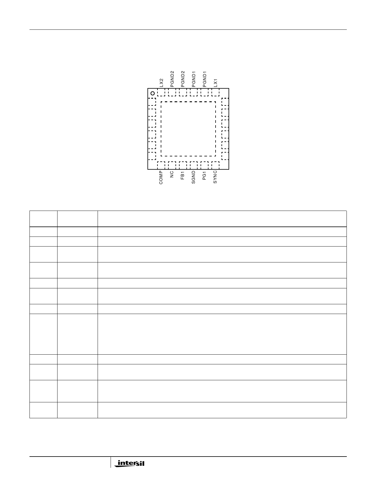
Pin Configuration
ISL8036, ISL8036A
ISL8036, ISL8036A
(24 LD QFN)
TOP VIEW
24 23 22 21 20 19
LX2 1
18 LX1
VIN2 2
17 VIN1
VIN2 3
EN2 4
25
PAD
16 VIN1
15 VDD
PG2 5
14 SS
FB2 6
13 EN1
7 8 9 10 11 12
Pin Descriptions
PIN
NUMBER
1, 24
22, 23
4
5
6
7
8
9
10
11
12
13
SYMBOL
LX2
PGND2
EN2
PG2
FB2
COMP
NC
FB1
SGND
PG1
SYNC
EN1
DESCRIPTION
Switching node connection for Channel 2. Connect to one terminal of inductor for VOUT2.
Negative supply for the power stage of Channel 2.
Regulator Channel 2 enable pin. Enable the output, VOUT2, when driven to high. Shutdown the
VOUT2 and discharge output capacitor when driven to low. Do not leave this pin floating.
1ms timer output. At power-up or EN HI, this output is a 1ms delayed Power-Good signal for the
VOUT2 voltage.
The feedback network of the Channel 2 regulator. To be connected to FB1 (current sharing)
An additional external network across COMP and SGND is required to improve the loop compensation
of the amplifier channel parallel operation. The soft-start pin should be tied to the external capacitor.
No connect pin; please tie to GND.
The feedback network of the Channel 1 regulator. FB1 is the negative input to the transconductance
error amplifier. The output voltage is set by an external resistor divider connected to FB1. With a
properly selected divider, the output voltage can be set to any voltage between the power rail
(reduced by converter losses) and the 0.8V reference. There is an internal compensation to meet a
typical application. In addition, the regulator power-good and undervoltage protection circuitry use
FB1 to monitor the Channel 1 regulator output voltage.
System ground.
1ms timer output. At power-up or EN HI, this output is a 1ms delayed Power-Good signal for the
VOUT1 voltage.
Connect to logic high or input voltage VIN . Connect to an external function generator for external
Synchronization. Negative edge trigger. Do not leave this pin floating. Do not tie this pin low (or
to SGND).
Regulator Channel 1 enable pin. Enable the output, VOUT1, when driven to high. Shutdown the
VOUT1 and discharge output capacitor when driven to low. Do not leave this pin floating.
5
FN6853.1
October 18, 2010
Share Link: 