IS3020 Просмотр технического описания (PDF) - Unspecified
Номер в каталоге
Компоненты Описание
производитель
IS3020 Datasheet PDF : 3 Pages
| |||
ELECTRICAL CHARACTERISTICS ( T = 25°C Unless otherwise noted )
A
PARAMETER
MIN TYP MAX UNITS
Input
Output
Forward Voltage (V )
F
Reverse Current (IR)
Peak Off-state Current ( I )
DRM
Peak Blocking Voltage ( VDRM )
On-state Voltage ( VTM )
Critical rate of rise of off-state
Voltage ( dv/dt ) ( note 1 )
Critical rate of rise of commutating
Voltage ( dv/dt ) ( note 1 )
1.2 1.5 V
100 µA
100 nA
400
V
1.5 3.0 V
10
V/µs
0.1 0.2
V/µs
TEST CONDITION
I = 10mA
F
VR = 6V
V = 400V (note 1 )
DRM
I = 100nA
DRM
ITM = 100mA ( peak )
I load = 15mA,
VIN = 30V ( fig 1. )
Coupled
Input Current to Trigger ( IFT )(note 2 )
IS3020
IS3021
IS3022
30 mA
15 mA
10 mA
Holding Current , either direction ( I )
H
100
µA
Input to Output Isolation Voltage VISO 5300
VRMS
7500
V
PK
VD = 3V ( note 2 )
See note 3
See note 3
Note 1. Test voltage must be applied within dv/dt rating.
Note 2. Guaranteed to trigger at an I value less than or equal to max. I , recommended I lies
F
FT
F
between Rated IFT and absolute max. IFT .
Note 3. Measured with input leads shorted together and output leads shorted together.
+5v
VCC
COMMUTATING
dv/dt
0v
STATIC
dv/dt
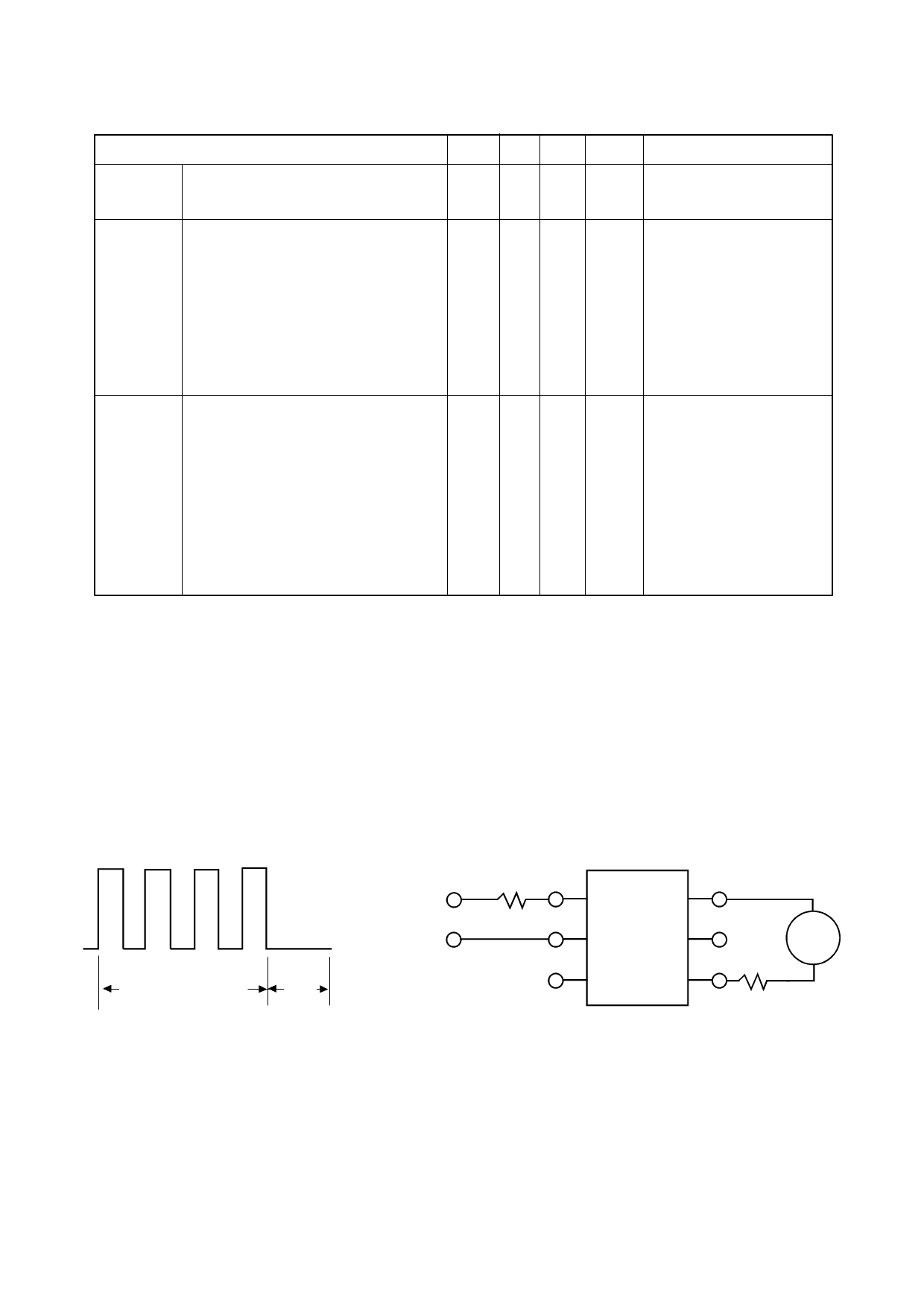
FIGURE 1
VCC
+
-
RIN
1
120Ω
2
3
6
5
4
RL
VIN
~
2kΩ
7/12/00
DB92284m-AAS/A1
Share Link: 