IS24C16-2 Просмотр технического описания (PDF) - Integrated Silicon Solution
Номер в каталоге
Компоненты Описание
производитель
IS24C16-2 Datasheet PDF : 11 Pages
| |||
IS24C16-2, IS24C16-3
IS24C08-2, IS24C08-3
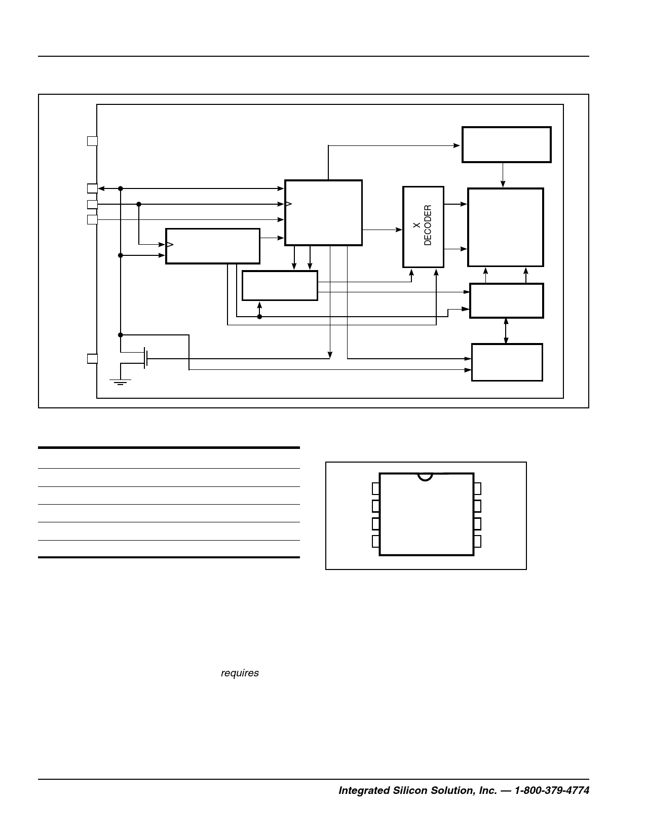
FUNCTIONAL BLOCK DIAGRAM
Vcc 8
SDA 5
SCL 6
WP 7
SLAVE ADDRESS
REGISTER &
COMPARATOR
CONTROL
LOGIC
WORD ADDRESS
COUNTER
GND 4
ACK
nMOS
ISSI ®
HIGH VOLTAGE
GENERATOR,
TIMING & CONTROL
EEPROM
ARRAY
Y
DECODER
Clock
DI/O
> DATA
REGISTER
PIN DESCRIPTIONS
A0-A2
Address Inputs
SDA
Serial Address/Data I/O
SCL
Serial Clock Input
WP
Write Protect Input
Vcc
Power Supply
GND
Ground
SCL
This input clock pin is used to synchronize the data
transfer to and from the device.
SDA
The SDA is a Bi-directional pin used to transfer addresses
and data into and out of the device. The SDA pin is an open
drain output and can be wire-Ored with other open drain or
open collector outputs. The SDA bus requires a pullup
resistor to Vcc.
A0, A1, A2
The A0, A1 and A2 are the device address inputs.
These pins are not used by IS24C16-2 and IS24C16-3.
A0 and A1 may be left floating or tied to either GND or Vcc.
A2 should be tied to either GND or Vcc.
2
PIN CONFIGURATION
8-Pin DIP and SOIC
A0 1
A1 2
A2 3
GND 4
8 VCC
7 WP
8 SCL
5 SDA
The IS24C08-2 and IS24C08-3 only use A2 input for
hardwire addressing and a total of two devices may be
addressed on a single bus system. The A0 and A1 pins are
not used by IS24C08-2 and IS24C08-3. They may be left
floating or tied to either GND or Vcc.
WP
WP is the Write Protect pin. If the WP pin is tied to Vcc the
upper half array becomes Write Protected (Read only).
When WP is tied to GND or left floating normal read/write
operations are allowed to the device.
Integrated Silicon Solution, Inc. — 1-800-379-4774
Rev. A
03/29/00
Share Link: 