CA5160M96(2003) Просмотр технического описания (PDF) - Intersil
Номер в каталоге
Компоненты Описание
производитель
CA5160M96
(Rev.:2003)
(Rev.:2003)
Intersil

CA5160M96 Datasheet PDF : 19 Pages
| |||
CA5160
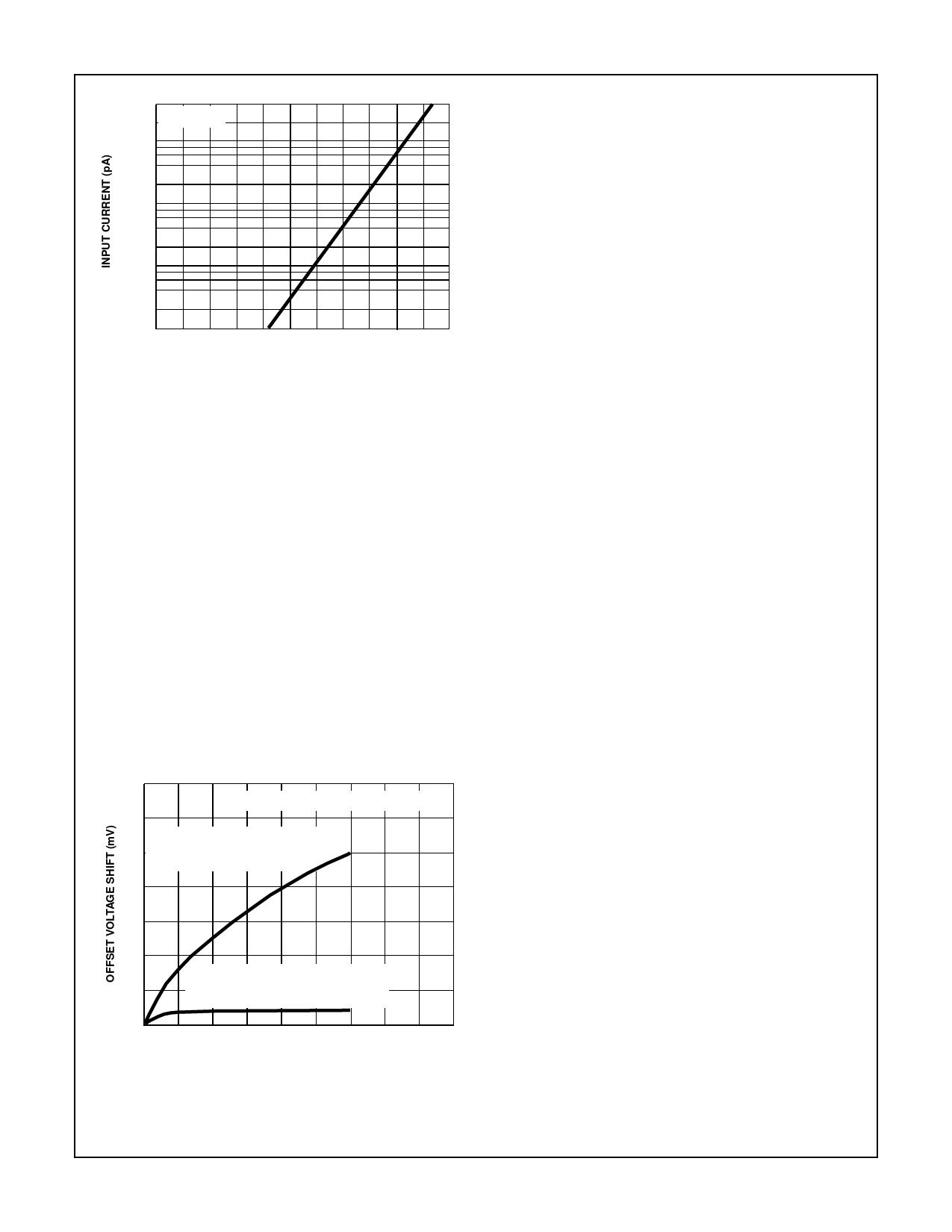
leakage current approximately doubles for every 10oC
increase in temperature. Figure 2 provides data on the
typical variation of input bias current as a function of
temperature in the CA5160.
In applications requiring the lowest practical input current
and incremental increases in current because of “warm-up”
effects, it is suggested that an appropriate heat sink be used
with the CA5160. In addition, when “sinking” or “sourcing”
significant output current the chip temperature increases,
causing an increase in the input current. In such cases, heat-
sinking can also very markedly reduce and stabilize input
current variations.
4000
1000
VS = ±7.5V
100
10
1
-80 -60 -40 -20 0 20 40 60 80 100 120 140
TEMPERATURE (oC)
FIGURE 2. INPUT CURRENT vs TEMPERATURE
Input Offset Voltage (VIO) Variation with DC Bias
vs Device Operating Life
It is well known that the characteristics of a MOSFET device
can change slightly when a DC gate-source bias potential is
applied to the device for extended time periods. The
magnitude of the change is increased at high temperatures.
Users of the CA5160 should be alert to the possible impacts
of this effect if the application of the device involves extended
operation at high temperatures with a significant differential
DC bias voltage applied across Terminals 2 and 3. Figure 3
shows typical data pertinent to shifts in offset voltage
encountered with CA5160 devices in metal can packages
during life testing. At lower temperatures (metal can and
plastic) for example at 85oC, this change in voltage is
considerably less. In typical linear applications where the
differential voltage is small and symmetrical, these
incremental changes are of about the same magnitude as
those encountered in an operational amplifier employing a
bipolar transistor input stage. The 2VDC differential voltage
example represents conditions when the amplifier output state
is “toggled”, e.g., as in comparator applications.
7
TA = 125oC FOR METAL CAN PACKAGES
6
DIFFERENTIAL DC VOLTAGE
5 (ACROSS TERMINALS 2 AND 3) = 2V
OUTPUT STAGE TOGGLED
4
3
2
DIFFERENTIAL DC VOLTAGE
1
(ACROSS TERMINALS 2 AND 3) = 0V
OUTPUT VOLTAGE = V+/2
0
0 500 1000 1500 2000 2500 3000 3500 4000
TIME (HOURS)
FIGURE 3. TYPICAL INCREMENTAL OFFSET VOLTAGE
SHIFT vs OPERATING LIFE
Power Supply Considerations
Because the CA5160 is very useful in single-supply
applications, it is pertinent to review some considerations
relating to power-supply current consumption under both
single-and dual-supply service. Figures 4A and 4B show the
CA5160 connected for both dual and single-supply
operation.
Dual-Supply Operation - When the output voltage at
Terminal 6 is 0V, the currents supplied by the two power
supplies are equal. When the gate terminals of Q8 and Q12
are driven increasingly positive with respect to ground,
current flow through Q12 (from the negative supply) to the
load is increased and current flow through Q8 (from the
positive supply) decreases correspondingly. When the gate
terminals of Q8 and Q12 are driven increasingly negative
with respect to ground, current flow through Q8 is increased
and current flow through Q12 is decreased accordingly.
Single Supply Operation - Initially, let it be assumed that the
value of RL is very high (or disconnected), and that the input-
terminal bias (Terminals 2 and 3) is such that the output
terminal (Number 6) voltage is at V+/2, i.e., the voltage-drops
across Q8 and Q12 are of equal magnitude. Figure 21 shows
typical quiescent supply-current vs supply-voltage for the
CA5160 operated under these conditions. Since the output
stage is operating as a Class A amplifier, the supply-current
will remain constant under dynamic operating conditions as
long as the transistors are operated in the linear portion of
their voltage transfer characteristics (see Figure 20). If either
Q8 or Q12 are swung out of their linear regions toward cutoff
(a nonlinear region), there will be a corresponding reduction in
supply-current. In the extreme case, e.g., with Terminal 8
swung down to ground potential (or tied to ground), NMOS
transistor Q12 is completely cut off and the supply-current to
series-connected transistors Q8, Q12 goes essentially to zero.
The two preceding stages in the CA5160, however, continue
7
Share Link: