LH28F400SUB-Z0 –ü—Ä–æ—Å–º–æ—Ç—Ä —Ç–µ—Ö–Ω–∏—á–µ—Å–∫–æ–≥–æ –æ–ø–∏—Å–∞–Ω–∏—è (PDF) - Sharp Electronics
–ù–æ–º–µ—Ä –≤ –∫–∞—Ç–∞–ª–æ–≥–µ
–ö–æ–º–ø–æ–Ω–µ–Ω—Ç—ã –û–ø–∏—Å–∞–Ω–∏–µ
–ø—Ä–æ–∏–∑–≤–æ–¥–∏—Ç–µ–ª—å
LH28F400SUB-Z0 Datasheet PDF : 34 Pages
| |||
4M (512K √ó 8, 256K √ó 16) Flash Memory
LH28F400SUB-Z0
When the device power-up or RP » turns High, Write
Protect Set/Confirm command must be written. Other-
wise, all lock bits in the device remain being locked,
can’t perform the Write to each block and single Block
Erase. Write Protect Set/Confirm command must be
written to reflect the actual lock status. However, when
the device power-on or RP » turns High, Erase All
Unlocked Blocks can be used. If used, Erase is per-
formed with reflecting actual lock status, and after that
Write and Block Erase can be used.
The LH28F400SU contains a Compatible Status
Register (CSR) which is 100% compatible with the
LH28F008SA Flash memory’s Status Register.This reg-
ister, when used alone, provides a straightforward
upgrade capability to the LH28F400SU from a
LH28F008SA-based design.
The LH28F400SU incorporates an open drain
RY »/BY » output pin. This feature allows the user to OR-
tie many RY/» BY» pins together in a multiple memory con-
figuration such as a Resident Flash Array.
The LH28F400SU is specified for a maximum
access time of 150 ns (tACC) at 3.3 V operation (3.0 to
3.6 V) over the extended temperature range (-20 to
+85°C). A corresponding maximum access time of
160 ns (tACC) at 2.7 V (-20 to +85°C) is achieved for
reduced power consumption applications.
The LH28F400SU incorporates an Automatic Power
Saving (APS) feature which substantially reduces the
active current when the device is in static mode of
operation (addresses not switching).
In APS mode, the typical ICC current is 1 mA at 3.3 V.
A Deep Power-Down mode of operation is invoked
when the RP » (called PWD on the LH28F008SA) pin
transitions low, any current operation is aborted and the
device is put into the deep power down mode. This mode
brings the device power consumption to less than 8 µA,
and provides additional write protection by acting as a
device reset pin during power transitions. When the
power is turned on, RP » pin is turned to low in order to
return the device to default configuration. When the
power transition is occurred, or at the power on/off, RP »
is required to stay low in order to protect data from noise.
A recovery time of 750 ns is required from RP » switch-
ing high until outputs are again valid. In the Deep Power-
Down state, the WSM is reset (any current operation
will abort) and the CSR register is cleared.
A CMOS Standby mode of operation is enabled when
CE » transitions high and RP » stays high with all input
control pins at CMOS levels. In this mode, the device
draws an ICC standby current of 15 µA.
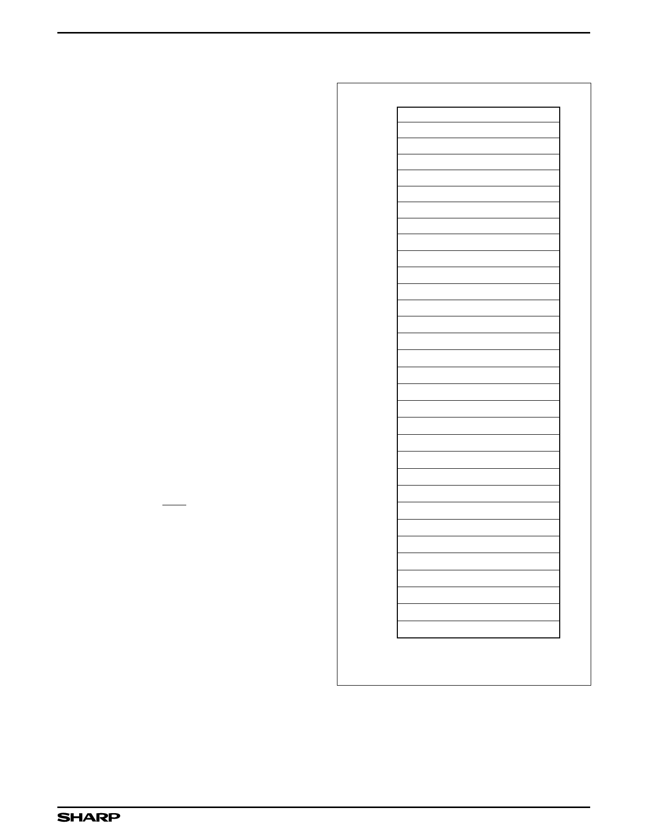
MEMORY MAP
7FFFFH
7C000H
7BFFFH
78000H
77FFFH
74000H
73FFFH
70000H
6FFFFH
6C000H
6BFFFH
68000H
67FFFH
64000H
63FFFH
60000H
5FFFFH
5C000H
5BFFFH
58000H
57FFFH
54000H
53FFFH
50000H
4FFFFH
4C000H
4BFFFH
48000H
47FFFH
44000H
43FFFH
40000H
3FFFFH
3C000H
3BFFFH
38000H
37FFFH
34000H
33FFFH
30000H
2FFFFH
2C000H
2BFFFH
28000H
27FFFH
24000H
23FFFH
20000H
1FFFFH
1C000H
1BFFFH
18000H
17FFFH
14000H
13FFFH
10000H
0FFFFH
0C000H
0BFFFH
08000H
07FFFH
04000H
03FFFH
00000H
16KB BLOCK
31
16KB BLOCK
30
16KB BLOCK
29
16KB BLOCK
28
16KB BLOCK
27
16KB BLOCK
26
16KB BLOCK
25
16KB BLOCK
24
16KB BLOCK
23
16KB BLOCK
22
16KB BLOCK
21
16KB BLOCK
20
16KB BLOCK
19
16KB BLOCK
18
16KB BLOCK
17
16KB BLOCK
16
16KB BLOCK
15
16KB BLOCK
14
16KB BLOCK
13
16KB BLOCK
12
16KB BLOCK
11
16KB BLOCK
10
16KB BLOCK
9
16KB BLOCK
8
16KB BLOCK
7
16KB BLOCK
6
16KB BLOCK
5
16KB BLOCK
4
16KB BLOCK
3
16KB BLOCK
2
16KB BLOCK
1
16KB BLOCK
0
NOTE: In Byte-wide (x8) mode A-1 is the lowest order address.
In Word-wide (x16) mode A-1 don't care, address values are
ignored A1.
28F400SUB-3
Figure 3. Memory Map
5
Share Link: 