FDS6670AS Просмотр технического описания (PDF) - Richtek Technology
Номер в каталоге
Компоненты Описание
производитель
FDS6670AS Datasheet PDF : 18 Pages
| |||
RT8298
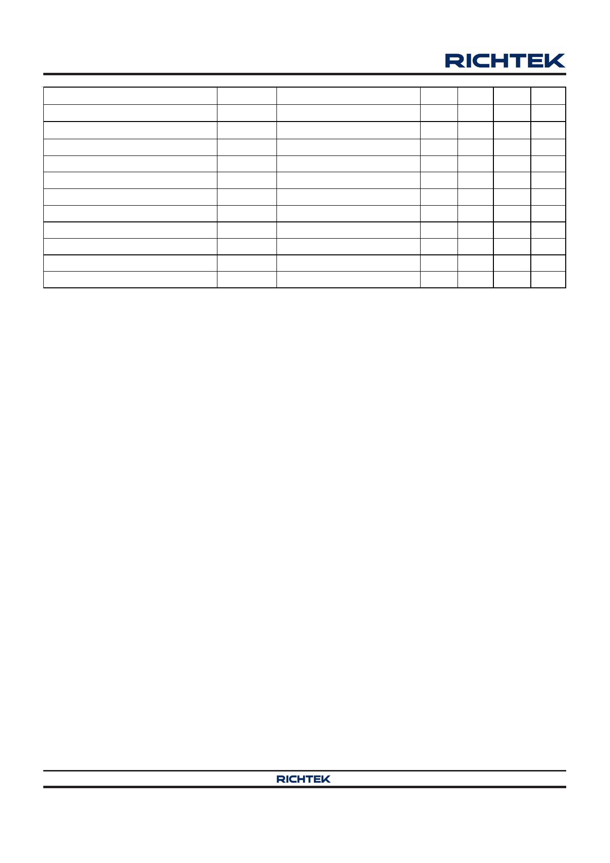
Parameter
Sync Frequency Range
EN Turn-Off Delay
EN Pull Low Current
Thermal Shutdown
Thermal Shutdown Hysteresis
Power Good Threshold Rising
Power Good Threshold Hysteresis
Power Good Pin Level
BG Driver Bias Supply Voltage
Gate Driver Sink Impedance
Gate Driver Source Impedance
Symbol
fSync
tOFF
TSD
ΔTSD
Test Conditions
VEN = 2V
VCC
RSink
RSource
PGOOD Sink 10mA
Min Typ Max Unit
0.3 -- 1.5 MHz
--
10
--
μs
--
1
-- μA
-- 150 --
°C
--
20
--
°C
-- 0.75 --
V
--
40
-- mV
--
-- 0.125 V
4.5 5
--
V
-- 0.9 --
Ω
-- 3.3 --
Ω
Note 1. Stresses beyond those listed “Absolute Maximum Ratings” may cause permanent damage to the device. These are
stress ratings only, and functional operation of the device at these or any other conditions beyond those indicated in the
operational sections of the specifications is not implied. Exposure to absolute maximum rating conditions may affect
device reliability.
Note 2. θJA is measured at TA = 25°C on a high effective thermal conductivity four-layer test board per JEDEC 51-7. θJC is
measured at the exposed pad of the package.
Note 3. Devices are ESD sensitive. Handling precaution is recommended.
Note 4. The device is not guaranteed to function outside its operating conditions.
Copyright ©2011 Richtek Technology Corporation. All rights reserved.
www.richtek.com
6
is a registered trademark of Richtek Technology Corporation.
DS8298-01 November 2011
Share Link: 