ILC6660 Просмотр технического описания (PDF) - Impala Linear Corporation
Номер в каталоге
Компоненты Описание
производитель
ILC6660 Datasheet PDF : 5 Pages
| |||
CMOS Monolithic Voltage Converter
Advance
V+
+
C1
1
FC
2
CAP+
8
V+
7
SYNC
3
ILC6660
VSS
6
LV
N/C
4
CAP-
5
VSH
C2
+
V+ (5V)
RL
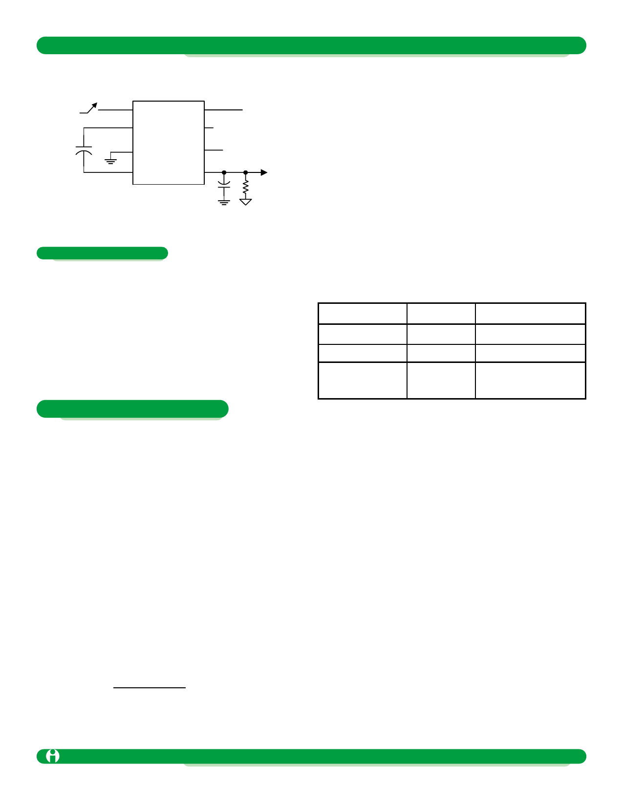
Figure 1: Test Circuit
For a nominal fPUMP of 5kHz and C2 = 100µF with an
ESR of 0.05Ω, ripple is approximately 100mV with a
100mA load current. If C2 is raised to 470µF, the ripple
drops to approximately 25mV.
Positive Voltage Doubler
The ILC6660 operates in the voltage-doubling mode as
shown in the Typical Circuit. The no-load output is 2 x VIN.
Positive Voltage Splitter
The ILC6660 operates in voltage splitting mode as shown in
the Typical Circuit. The no-load output is VIN/2
Detailed Description
The ILC6660 capacitive charge-pump circuit either
inverts, splits or doubles the input voltage (see Typical
Circuits). For highest performance, low effective series
resistance (ESR) capacitors should be used (see
Capacitor Selection section for more details). When using
the inverting mode with a supply voltage less than 2V, LV
may be connected to VSS. This bypasses the internal
regulator circuitry and provides best performance in low-
voltage applications. When using the inverter mode with
a supply voltage above 2V, LV must be left open.
Changing Oscillator Frequency
Three modes control the ILC6660's clock frequency,
as listed below:
FC
Open
FC = V+
Open
SYNC
Open
Open
External
Clock
Oscillator Frequency
5kHz
50kHz
External Clock
Frequency
Applications Information
Negative Voltage Converter
The most common application of the ILC6660 is as a
charge-pump voltage inverter. The operating circuit uses
only two external capacitors, C1 and C2 (see Typical
Circuits). Even though its output is not actively regulated,
the ILC6660 is very insensitive to load current changes. A
typical output source resistance of 5Ω means that with an
input of +5V the output voltage is -5V under light load, and
decreases only to 4.5V with a load of 100mA.
Capacitors selection
Low ESR capacitors should be used at the output of
ILC6660 to minimize output ripple. This can be achieved
using ceramic capacitors, but may also be met with certain
types of tantalum capacitors.
Output ripple voltage is calculated taking into account that
the output current is solely supplied from capacitor C2 dur-
ing one-half of the charge-pump cycle. This introduces a
peak-to-peak ripple of:
When FC and SYNC are unconnected (open), the
Oscillator runs at 5kHz typically. When FC is connected to
V+, the charge and discharge current change from 1.0µA
to 10.0µA, thus increasing the Oscillator frequency 10
times. In the inverter mode, SYNC may also be overdriv-
en by an external clock source. A square wave signal of
maximum 2V peak-to-peak may be applied to SYNC via
a 2…5nF capacitor to overdrive the internal oscillator.
When SYNC is overdriven, FC has no effect. In some
applications, the 5kHz output ripple frequency may be low
enough to interfere with other circuitry. If desired, the
Oscillator frequency can then be increased through use of
the FC pin or an external Oscillator as described above.
Increasing the clock frequency increases the ILC6660's
quiescent current, but also allows smaller capacitance val-
ues to be used for C1 and C2.
V RIPPLE =
I VSH
+ I VSH (ESRC2)
2(f PUMP)(C2)
Impala Linear Corporation
ILC6660 1.8
(408) 574-3939 www.impalalinear.com
May 2000 4
Share Link: 