IDT72V3672L15PQF(2003) Просмотр технического описания (PDF) - Integrated Device Technology
Номер в каталоге
Компоненты Описание
производитель
IDT72V3672L15PQF Datasheet PDF : 29 Pages
| |||
IDT72V3652/72V3662/72V3672 3.3V CMOS SyncBiFIFOTM
2,048 x 36 x 2, 4,096 x 36 x 2 and 8,192 x 36 x 2
COMMERCIAL TEMPERATURE RANGE
ABSOLUTE MAXIMUM RATINGS OVER OPERATING FREE-AIR
TEMPERATURE RANGE (Unless otherwise noted)(1)
Symbol
Rating
Commercial
Unit
VCC
Supply Voltage Range
–0.5 to +4.6
V
VI(2)
Input Voltage Range
–0.5 to VCC+0.5
V
VO(2)
Output Voltage Range
–0.5 to VCC+0.5
V
IIK
Input Clamp Current (VI < 0 or VI > VCC)
±20
mA
IOK
Output Clamp Current (VO = < 0 or VO > VCC)
±50
mA
IOUT
Continuous Output Current (VO = 0 to VCC)
±50
mA
ICC
Continuous Current Through VCC or GND
±400
mA
TSTG
Storage Temperature Range
–65 to 150
°C
NOTES:
1. Stresses beyond those listed under "Absolute Maximum Ratings" may cause permanent damage to the device. These are stress ratings only and functional operation of the device at these
or any other conditions beyond those indicated under "recommended operating conditions" is not implied. Exposure to absolute maximum rated conditions for extended periods may affect
device reliability.
2. The input and output voltage ratings may be exceeded provided the input and output current ratings are observed.
RECOMMENDED OPERATING CONDITIONS
Symbol
Parameter
Min. Typ. Max. Unit
VCC(1) Supply Voltage for 10ns
3.15 3.3
3.45
V
VCC
Supply Voltage for 15ns
3.0 3.3
3.6
V
VIH
High-Level Input Voltage
2
— VCC+0.5 V
VIL
Low-Level Input Voltage
——
0.8
V
IOH
High-Level Output Current
——
–4
mA
IOL
Low-Level Output Current
——
8
mA
TA
Operating Temperature
0
—
70
°C
NOTE:
1. For 10ns speed grade: Vcc = 3.3V ± 0.15V, JEDEC JESD8-A compliant
ELECTRICAL CHARACTERISTICS OVER RECOMMENDED OPERATING
FREE-AIR TEMPERATURE RANGE (Unless otherwise noted)
Symbol
Parameter
VOH Output Logic "1" Voltage
VOL Output Logic "0" Voltage
ILI
Input Leakage Current (Any Input)
ILO
Output Leakage Current
ICC2(3) Standby Current (with CLKA & CLKB running)
ICC3(3) Standby Current (no clocks running)
CIN(4) InputCapacitance
COUT(4) OutputCapacitance
VCC = 3.0V,
VCC = 3.0V,
VCC = 3.6V,
VCC = 3.6V,
VCC = 3.6V,
VCC = 3.6V,
VI = 0,
VO = 0,
Test Conditions
IOH = –4 mA
IOL = 8 mA
VI = VCC or 0
VO = VCC or 0
VI = VCC –0.2V or 0V
VI = VCC –0.2V or 0V
f = 1 MHz
f = 1 MHZ
IDT72V3652
IDT72V3662
IDT72V3672
Commercial
tCLK = 10, 15 ns(2)
Min. Typ.(1) Max. Unit
2.4
—
—
V
—
—
0.5
V
—
—
±10
µA
—
—
±10
µA
—
—
5
mA
—
—
1
mA
—
4
—
pF
—
8
—
pF
NOTES:
1. All typical values are at VCC = 3.3V, TA = 25°C.
2. Commercial-10ns speed grade only: Vcc = 3.3V ± 0.15V, TA = 0° to +70°; JEDEC JESD8-A compliant.
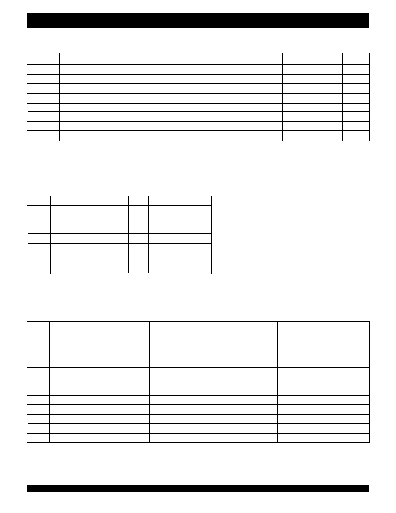
3. For additional ICC information, see Figure 1, Typical Characteristics: Supply Current (ICC) vs. Clock Frequency (fS).
4. Characterized values, not currently tested.
6
Share Link: 