ICS854054 Просмотр технического описания (PDF) - Integrated Circuit Systems
Номер в каталоге
Компоненты Описание
производитель
ICS854054 Datasheet PDF : 13 Pages
| |||
Integrated
Circuit
Systems, Inc.
ICS854054
4:1
DIFFERENTIAL-TO-LVDS CLOCK MULTIPLEXER
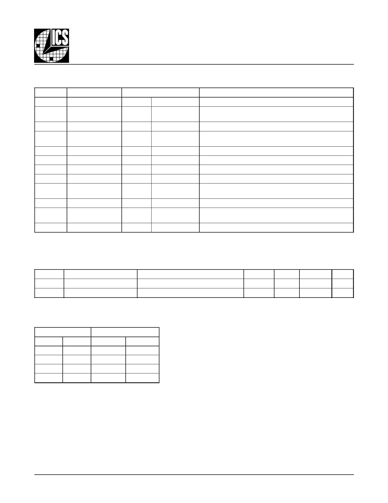
TABLE 1. PIN DESCRIPTIONS
Number
Name
Type
Description
1
PCLK0
Input
Pulldown Non-inverting differential clock input.
2
nPCLK0
Input
Pullup/Pulldown
Inverting differential clock input.
VDD/2 default when left floating.
3
PCLK1
Input
Pulldown Non-inverting differential clock input.
4
5, 16
6, 7
nPCLK1
V
DD
SEL0, SEL1
Input
Power
Input
Pullup/Pulldown
Inverting differential clock input.
V /2 default when left floating.
DD
Positive supply pins.
Pulldown Clock select input pins. LVCMOS/LVTTL interface levels.
8, 13
GND
Power
Power supply ground.
9
PCLK2
Input
Pulldown Non-inverting differential clock input.
10
nPCLK2
Input
Pullup/Pulldown
Inverting differential clock input.
VDD/2 default when left floating.
11
PCLK3
Input
Pulldown Non-inverting differential clock input.
12
14, 15
nPCLK3
nQ0, Q0
Input
Output
Pullup/Pulldown
Inverting differential clock input.
VDD/2 default when left floating.
Differential output pair. LVDS interface levels.
NOTE: Pullup and Pulldown refer to internal input resistors. See Table 2, Pin Characteristics, for typical values.
TABLE 2. PIN CHARACTERISTICS
Symbol
RPULLDOWN
RVDD/2
Parameter
Pulldown Resistor
Pullup/Pulldown Resistors
Test Conditions
Minimum
Typical
75
50
Maximum
Units
kΩ
kΩ
TABLE 3. CLOCK INPUT FUNCTION TABLE
Inputs
SEL1 SEL0
0
0
0
1
1
0
1
1
Outputs
Q
nQ
PCLK0 nPCLK0
PCLK1 nPCLK1
PCLK2 nPCLK2
PCLK3 nPCLK3
854054AG
www.icst.com/products/hiperclocks.html
2
REV. A MARCH 29, 2006
Share Link: 