HGTG11N120CND Просмотр технического описания (PDF) - Fairchild Semiconductor
Номер в каталоге
Компоненты Описание
производитель
HGTG11N120CND
Fairchild Semiconductor

HGTG11N120CND Datasheet PDF : 8 Pages
| |||
HGTG11N120CND
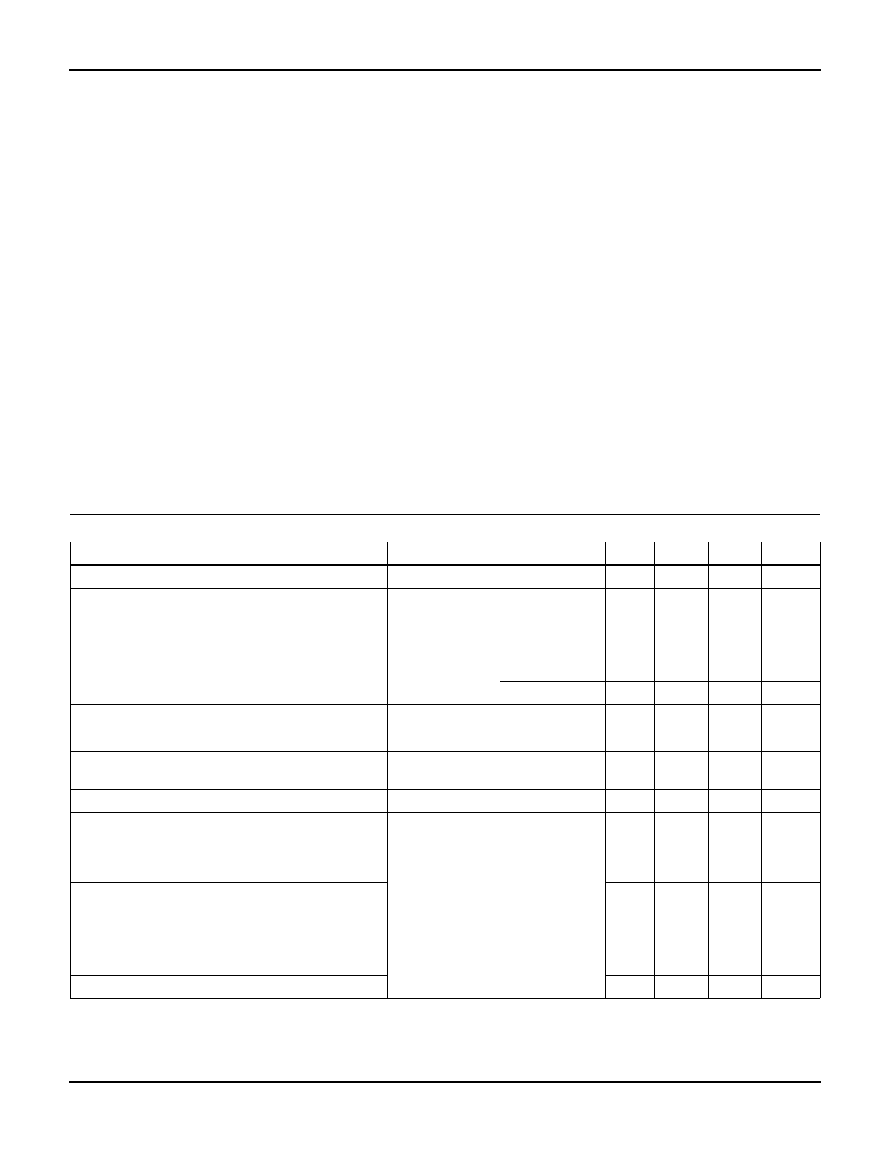
Absolute Maximum Ratings TC = 25oC, Unless Otherwise Specified
Collector to Emitter Voltage . . . . . . . . . . . . . . . . . . . . . . . . . . . . . . . . . . . . . . . . . . . . . .BVCES
Collector Current Continuous
At TC = 25oC . . . . . . . . . . . . . . . . . . . . . . . . . . . . . . . . . . . . . . . . . . . . . . . . . . . . . . . . . IC25
At TC = 110oC . . . . . . . . . . . . . . . . . . . . . . . . . . . . . . . . . . . . . . . . . . . . . . . . . . . . . . . IC110
Collector Current Pulsed (Note 1) . . . . . . . . . . . . . . . . . . . . . . . . . . . . . . . . . . . . . . . . . . . ICM
Gate to Emitter Voltage Continuous. . . . . . . . . . . . . . . . . . . . . . . . . . . . . . . . . . . . . . . . . VGES
Gate to Emitter Voltage Pulsed . . . . . . . . . . . . . . . . . . . . . . . . . . . . . . . . . . . . . . . . . . . .VGEM
Switching Safe Operating Area at TJ = 150oC (Figure 2) . . . . . . . . . . . . . . . . . . . . . . . SSOA
Power Dissipation Total at TC = 25oC . . . . . . . . . . . . . . . . . . . . . . . . . . . . . . . . . . . . . . . . . PD
Power Dissipation Derating TC > 25oC . . . . . . . . . . . . . . . . . . . . . . . . . . . . . . . . . . . . . . . . . .
Operating and Storage Junction Temperature Range . . . . . . . . . . . . . . . . . . . . . . . . TJ, TSTG
Maximum Lead Temperature for Soldering . . . . . . . . . . . . . . . . . . . . . . . . . . . . . . . . . . . . . TL
Short Circuit Withstand Time (Note 2) at VGE = 15V . . . . . . . . . . . . . . . . . . . . . . . . . . . . . .tSC
Short Circuit Withstand Time (Note 2) at VGE = 12V . . . . . . . . . . . . . . . . . . . . . . . . . . . . . .tSC
HGTG11N120CND
1200
43
22
80
±20
±30
55A at 1200V
298
2.38
-55 to 150
260
8
15
UNITS
V
A
A
A
V
V
W
W/oC
oC
oC
µs
µs
CAUTION: Stresses above those listed in “Absolute Maximum Ratings” may cause permanent damage to the device. This is a stress only rating and operation of the
device at these or any other conditions above those indicated in the operational sections of this specification is not implied.
NOTES:
1. Pulse width limited by maximum junction temperature.
2. VCE(PK) = 840V, TJ = 125oC, RG = 10Ω.
Electrical Specifications TC = 25oC, Unless Otherwise Specified
PARAMETER
SYMBOL
TEST CONDITIONS
Collector to Emitter Breakdown Voltage
Collector to Emitter Leakage Current
Collector to Emitter Saturation Voltage
Gate to Emitter Threshold Voltage
Gate to Emitter Leakage Current
Switching SOA
BV CES
I CES
VCE(SAT)
VGE(TH)
IGES
SSOA
IC = 250µA, VGE = 0V
VCE = 1200V
TC = 25oC
TC = 125oC
TC = 150oC
IC = 11A,
VGE = 15V
TC = 25oC
TC = 150oC
IC = 90µA, VCE = VGE
VGE = ±20V
TJ = 150oC, RG = 10Ω, VGE = 15V,
L = 400µH, VCE(PK) = 1200V
Gate to Emitter Plateau Voltage
On-State Gate Charge
Current Turn-On Delay Time
Current Rise Time
Current Turn-Off Delay Time
Current Fall Time
Turn-On Energy
Turn-Off Energy (Note 3)
VGEP
QG(ON)
td(ON)I
trI
td(OFF)I
tfI
EON
EOFF
IC = 11A, VCE = 600V
IC = 11A,
VCE = 600V
VGE = 15V
VGE = 20V
IGBT and Diode at TJ = 25oC,
ICE = 11A,
VCE = 960V,
VGE = 15V,
RG = 10Ω,
L = 2mH,
Test Circuit (Figure 20)
MIN TYP
1200
-
-
-
-
300
-
-
-
2.1
-
2.9
6.0
6.8
-
-
55
-
MAX
-
250
-
3.5
2.4
3.5
-
±250
-
UNITS
V
µA
µA
mA
V
V
V
nA
A
-
10.4
-
V
-
100
120
nC
-
130
150
nC
-
23
26
ns
-
12
16
ns
-
180
240
ns
-
190
220
ns
-
0.95
1.3
mJ
-
1.3
1.6
mJ
©2001 Fairchild Semiconductor Corporation
HGTG11N120CND Rev. B
Share Link: