ICL3237 Просмотр технического описания (PDF) - Intersil
Номер в каталоге
Компоненты Описание
производитель
ICL3237 Datasheet PDF : 11 Pages
| |||
ICL3237
Detailed Description
The ICL3237 operates from a single +3V to +5.5V supply,
guarantees a 1Mbps minimum data rate, requires only four
small external 0.1µF capacitors, features low power
consumption, and meets all EIA/TIA-232 and V.28
specifications. The circuit is divided into three sections: The
charge pump, the transmitters, and the receivers.
Charge-Pump
Intersil’s new ICL32XX family utilizes regulated on-chip dual
charge pumps as voltage doublers, and voltage inverters to
generate ±5.5V transmitter supplies from a VCC supply as
low as 3.0V. This allows these devices to maintain RS-232
compliant output levels over the ±10% tolerance range of
3.3V powered systems. The efficient on-chip power supplies
require only four small, external 0.1µF capacitors for the
voltage doubler and inverter functions at VCC = 3.3V. See
the “Capacitor Selection” section, and Table 3 for capacitor
recommendations for other operating conditions. The charge
pumps operate discontinuously (i.e., they turn off as soon as
the V+ and V- supplies are pumped up to the nominal
values), resulting in significant power savings.
Transmitters
The transmitters are proprietary, low dropout, inverting
drivers that translate TTL/CMOS inputs to EIA/TIA-232
output levels. Coupled with the on-chip ±5.5V supplies,
these transmitters deliver true RS-232 levels over a wide
range of single supply system voltages.
All transmitter outputs disable and assume a high impedance
state when the device enters the powerdown mode (see Table
2). These outputs may be driven to ±12V when disabled.
The ICL3237 guarantees a 1Mbps data rate (if MBAUD = 1)
for full load conditions (3kΩ and 250pF), VCC ≥ 3.0V, with
one transmitter operating at full speed. Under more typical
conditions of VCC ≥ 3.3V, C1-4 = 0.1µF, RL = 3kΩ, and
CL = 250pF, one transmitter easily operates at 1.7Mbps.
Transmitter inputs float if left unconnected, and may cause
ICC increases. Connect unused inputs to GND for the best
performance.
Receivers
The ICL3237 device contains standard inverting receivers
that three-state only when the EN control line is driven high.
Additionally, it includes a noninverting (monitor) receiver
(denoted by the ROUTB label) that is always active,
regardless of the state of any control lines. All the receivers
convert RS-232 signals to CMOS output levels and accept
inputs up to ±25V while presenting the required 3kΩ to 7kΩ
input impedance (see Figure 1) even if the power is off
(VCC = 0V). The receivers’ Schmitt trigger input stage uses
hysteresis to increase noise immunity and decrease errors
due to slow input signal transitions.
Monitor receivers remain active even during manual
powerdown and forced receiver disable, making them
extremely useful for Ring Indicator monitoring. Standard
receivers driving powered down peripherals must be disabled
to prevent current flow through the peripheral’s protection
diodes (see Figures 2 and 3). This renders them useless for
wake up functions, but the corresponding monitor receiver
can be dedicated to this task as shown in Figure 3.
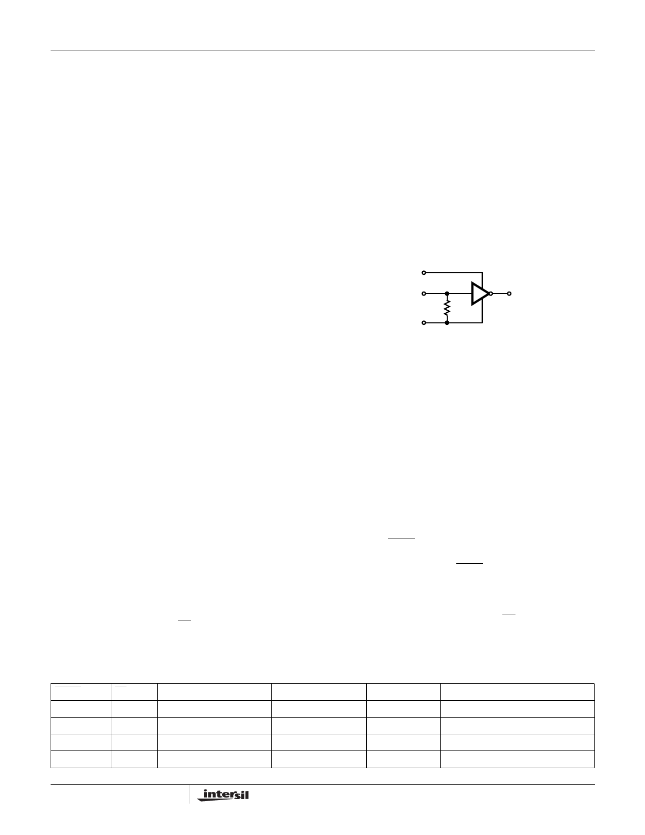
VCC
RXIN
-25V ≤ VRIN ≤ +25V 5kΩ
GND
RXOUT
GND ≤ VROUT ≤ VCC
FIGURE 1. INVERTING RECEIVER CONNECTIONS
Powerdown Functionality
This 3V device requires a nominal supply current of 0.3mA
during normal operation (not in powerdown mode). This is
considerably less than the 5mA to 11mA current required of
5V RS-232 devices. The already low current requirement
drops significantly when the device enters powerdown
mode. In powerdown, supply current drops to 1µA, because
the on-chip charge pump turns off (V+ collapses to VCC, V-
collapses to GND), and the transmitter outputs three-state.
This micro-power mode makes the ICL3237 ideal for battery
powered and portable applications.
Software Controlled (Manual) Powerdown
On the ICL3237, the powerdown control is via a simple
shutdown (SHDN) pin. Driving this pin high enables normal
operation, while driving it low forces the IC into it’s
powerdown state. Connect SHDN to VCC if the powerdown
function isn’t needed. Note that all the receiver outputs
remain enabled during shutdown (see Table 2). For the
lowest power consumption during powerdown, the receivers
should also be disabled by driving the EN input high (see
next section, and Figures 2 and 3). The time required to exit
powerdown, and resume transmission is only 100µs.
TABLE 2. POWERDOWN AND ENABLE LOGIC TRUTH TABLE
SHDN INPUT EN INPUT TRANSMITTER OUTPUTS RECEIVER OUTPUTS ROUTB OUTPUT
MODE OF OPERATION
L
L
High-Z
Active
Active
Manual Powerdown
L
H
High-Z
High-Z
Active
Manual Powerdown w/Rcvr. Disabled
H
L
Active
Active
Active
Normal Operation
H
H
Active
High-Z
Active
Normal Operation w/Rcvr. Disabled
6
Share Link: 