HT66FU50 Просмотр технического описания (PDF) - Holtek Semiconductor
Номер в каталоге
Компоненты Описание
производитель
HT66FU50 Datasheet PDF : 246 Pages
| |||
HT66F20/HT66F30/HT66F40/HT66F50/HT66F60
HT66FU30/HT66FU40/HT66FU50/HT66FU60
Note:
I/T: Input type; O/T: Output type
OP: Optional by configuration option (CO) or register option
PWR: Power; CO: Configuration option; ST: Schmitt Trigger input
CMOS: CMOS output; NMOS: NMOS output
SCOM: Software controlled LCD COM; AN: Analog input pin
HXT: High frequency crystal oscillator
LXT: Low frequency crystal oscillator
*: VDD is the device power supply while AVDD is the ADC power supply. The AVDD pin is bonded together
internally with VDD.
**: VSS is the device ground pin while AVSS is the ADC ground pin. The AVSS pin is bonded together
internally with VSS.
As the Pin Description Summary table applies to the package type with the most pins, not all of the above listed
pins may be present on package types with smaller numbers of pins.
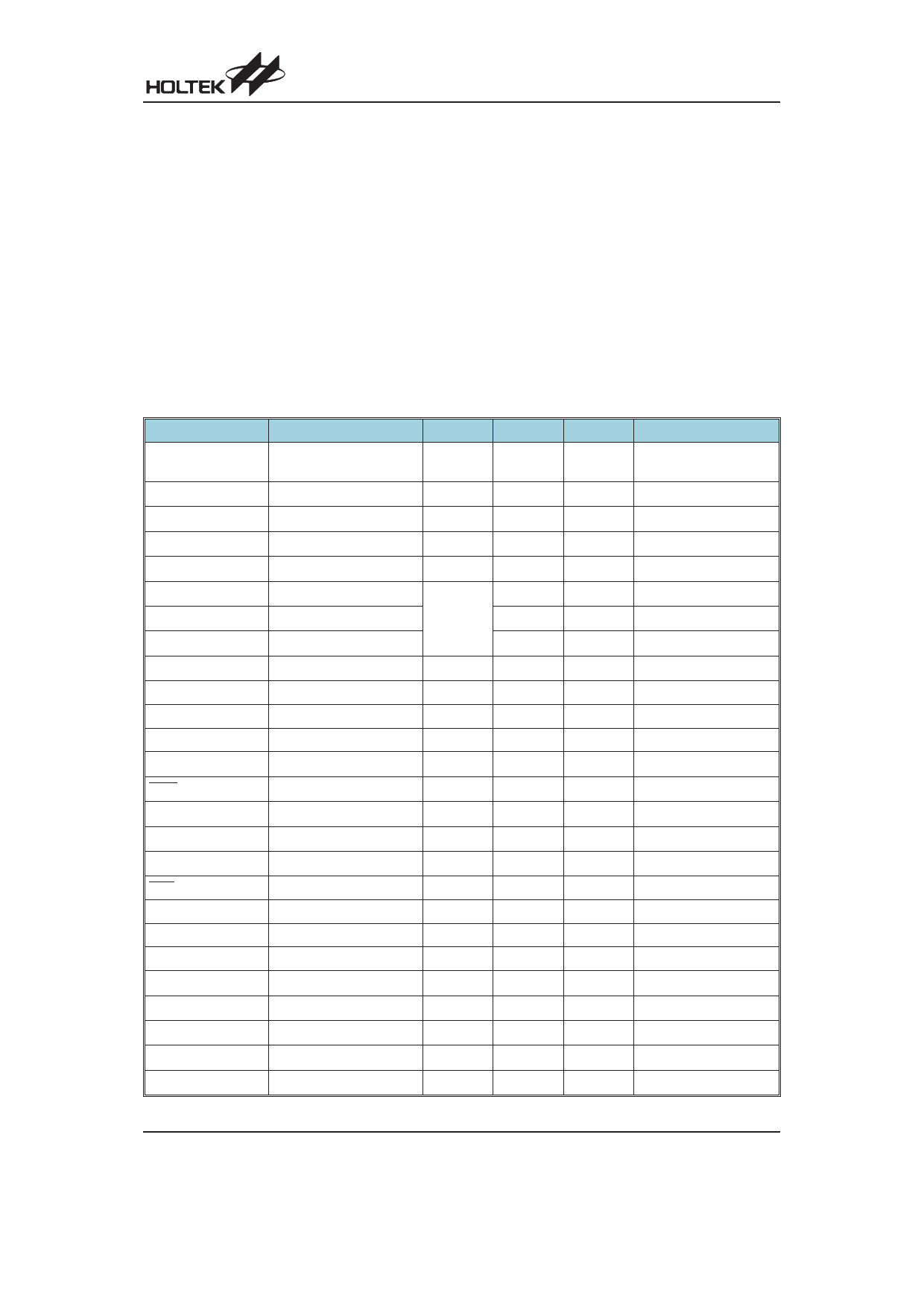
HT66F30
Pin Name
PA0~PA7
PB0~PB5
PC0~PC7
AN0~AN7
VREF
C0-, C1-
C0+, C1+
C0X, C1X
TCK0, TCK1
TP0_0, TP0_1
TP1A
TP1B_0, TP1B_1
INT0, INT1
PINT
PCK
SDI
SDO
SCS
SCK
SCL
SDA
SCOM0~SCOM3
OSC1
OSC2
XT1
XT2
Function
Port A
Port B
Port C
ADC input
ADC reference input
Comparator 0, 1 input
Comparator 0, 1 input
Comparator 0, 1 output
TM0, TM1 input
TM0 I/O
TM1 I/O
TM1 I/O
Ext. Interrupt 0, 1
Peripheral Interrupt
Peripheral Clock output
SPI Data input
SPI Data output
SPI Slave Select
SPI Serial Clock
I2C Clock
I2C Data
SCOM0~SCOM3
HXT/ERC pin
HXT pin
LXT pin
LXT pin
OP
PAWU
PAPU
PBPU
PCPU
ACERL
ADCR1
CP0C
CP1C
¾
TMPC0
TMPC0
TMPC0
¾
PRM0
PRM0
PRM0
PRM0
PRM0
PRM0
PRM0
PRM0
SCOMC
CO
CO
CO
CO
I/T
ST
ST
ST
AN
AN
AN
AN
¾
ST
ST
ST
ST
ST
ST
¾
ST
¾
ST
ST
ST
ST
¾
HXT
¾
LXT
¾
O/T
Pin-Shared Mapping
CMOS ¾
CMOS
CMOS
¾
¾
¾
¾
CMOS
¾
CMOS
CMOS
CMOS
¾
¾
CMOS
¾
CMOS
CMOS
CMOS
NMOS
NMOS
SCOM
¾
HXT
¾
LXT
¾
¾
PA0~PA7
PB5
PA3, PC3
PA2, PC2
PA0, PA5
PA2, PA4
PA0, PC5
PA1
PC0, PC1
PA3, PA4
PC3 or PC4
PC2 or PC5
PA6 or PC0
PA5 or PC1
PB5 or PC6
PA7 or PC7
PA7 or PC7
PA6 or PC0
PC0, PC1, PC6, PC7
PB1
PB2
PB3
PB4
Rev. 1.10
8
February 1, 2010
Share Link: 