AD584SH(Rev_A) Просмотр технического описания (PDF) - Analog Devices
Номер в каталоге
Компоненты Описание
производитель
AD584SH Datasheet PDF : 8 Pages
| |||
AD584
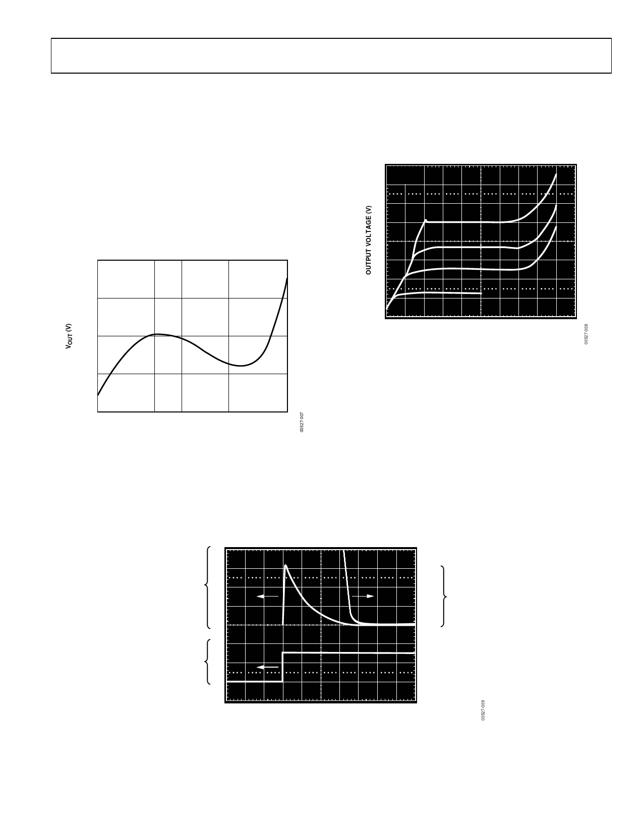
istics and long-term stability of the device will be essentially the
same as that of a unit used in the standard three-terminal mode.
age ranges. For example, a +10 V reference produces a 0 V to
–10 V range. If an AD308 amplifier is used, total quiescent sup-
ply current will typically be 2 mA. The AD584 will normally be
used in the –10 volt mode with the AD7574 to give a 0 volt to
+10 volt ADC range. This is shown in Figure 16. Bipolar out-
put applications and other operating details can be found in the
data sheets for the CMOS products.
Figure 13. Two-Terminal –5 Volt Reference
The AD584 can also be used in a two-terminal mode to develop
a positive reference. VIN and VOUT are tied together and to the
positive supply through an appropriate supply resistor. The per-
formance characteristics will be similar to those of the negative
two-terminal connection. The only advantage of this connection
over the standard three-terminal connection is that a lower pri-
mary supply can be used, as low as 0.5 volts above the desired
output voltage. This type of operation will require considerable
attention to load and primary supply regulation to be sure the
AD584 always remains within its regulating range of 1 mA to
5 mA (2 mA to 5 mA for operation beyond 85°C).
10 VOLT REFERENCE WITH MULTIPLYING CMOS D/A
OR A/D CONVERTERS
The AD584 is ideal for application with the entire AD7520
series of 10- and 12-bit multiplying CMOS D/A converters,
especially for low power applications. It is equally suitable for
the AD7574 8-bit A/D converter. In the standard hook-up as
shown in Figure 14, the standard output voltages are inverted
by the amplifier/DAC configuration to produce converted volt-
Figure 14. Low Power 10-Bit CMOS DAC Application
PRECISION D/A CONVERTER REFERENCE
The AD562, like many D/A converters, is designed to operate
with a +10 volt reference element (Figure 15). In the AD562,
this 10 volt reference voltage is converted into a reference cur-
rent of approximately 0.5 mA via the internal 19.95 kΩ resistor
(in series with the external 100 Ω trimmer). The gain tempera-
ture coefficient of the AD562 is primarily governed by the tem-
perature tracking of the 19.95 kΩ resistor and the 5k/10k span
resistors; this gain T.C. is guaranteed to 3 ppm/°C. Thus, using
the AD584L (at 5 ppm/°C) as the 10 volt reference guarantees a
REV. A
Figure 15. Precision 12-Bit D/A Converter
–7–
Share Link: 