HT46R652-100 Просмотр технического описания (PDF) - Holtek Semiconductor
Номер в каталоге
Компоненты Описание
производитель
HT46R652-100 Datasheet PDF : 47 Pages
| |||
HT46R652
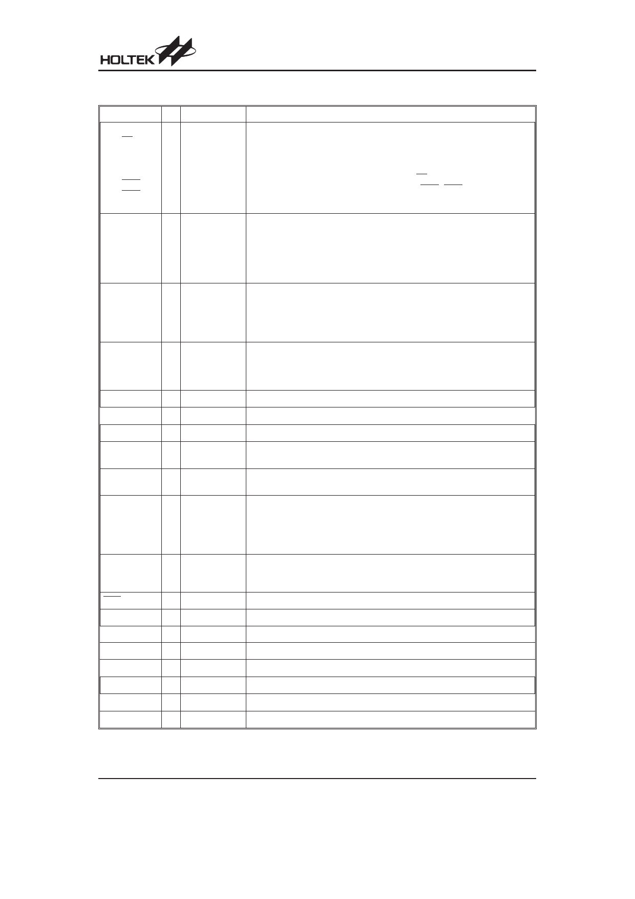
Pin Description
Pin Name I/O Options
Description
PA0/BZ
PA1/BZ
PA2
PA3/PFD
PA4/TMR0
PA5/INT0
PA6/INT1
PA7/TMR1
I/O
Wake-up
Pull-high
Buzzer
PFD
Bidirectional 8-bit input/output port. Each individual pin on this port can be
configured as a wake-up input by a configuration option. Software instruc-
tions determine if the pin is a CMOS output or Schmitt trigger input. Configu-
ration options determine which pins on the port have pull-high resistors. Pins
PA0, PA1 and PA3 are pin-shared with BZ, BZ and PFD respectively. Pins
PA5, PA6, PA4 and PA7 are pin-shared with INT0, INT1, TMR0 and TMR1
respectively.
Bidirectional 8-bit input/output port. Software instructions determine if the pin
is a CMOS output or Schmitt trigger input. Configuration options determine
PB0/AN0~
PB7/AN7
I/O
Pull-high
which pins on the port have pull-high resistors. PB is pin-shared with the A/D
input pins. The A/D inputs are selected via software instructions. Once a PB
line is selected as an A/D input, the I/O function and pull-high resistor
functions are disabled automatically.
PC0/PWM0~
PC7/PWM7
I/O
Pull-high
PWM
Bidirectional 8-bit input/output port. Software instructions determine if the pin
is a CMOS output or Schmitt trigger input. Configuration options determine if
all pins on the port have pull-high resistors. A configuration option deter-
mines if all of the pins on this port are to be used as PWM outputs. Individual
pins cannot be selected to have a PWM function.
PD0/PWM8~
PD7/PWM15
I/O
Pull-high
PWM
Bidirectional 8-bit input/output port. Software instructions determine if the pin
is a CMOS output or Schmitt trigger input. Configuration options determine
which pins on the port have pull-high resistors. A configuration option for
each pin on this port determines if each pin is to be used as a PWM output.
VLCD
I
¾
LCD power supply
VMAX
I
¾
IC maximum voltage connect to VDD, VLCD or V1
V1, V2, C1, C2 I
¾
Voltage pump
COM0~COM2
COM3/SEG40
O
1/3 or 1/4 Duty
SEG40 can be set as a segment or as a common output driver for LCD panel
by options. COM0~COM2 are outputs for the LCD panel.
SEG0~SEG39 O
Logical Output
LCD driver outputs for the the LCD panel segments. SEG0~SEG23 can be
configured as logical outputs via a configuration option.
OSC1
OSC2
OSC1 and OSC2 are connected to an RC network or external crystal (deter-
I
O
mined by a configuration option) for the internal system clock. If the RC sys-
Crystal or RC tem clock is selected, OSC2 can be used to measure the system clock at 1/4
frequency. The system clock may also be sourced from the RTC oscillator, in
which case these two pins can be left floating.
OSC3
OSC4
I
O
RTC or
System Clock
Real time clock oscillator. OSC3 and OSC4 are connected to a 32768Hz
crystal oscillator for timing purposes or to form a system clock source, de-
pending on configuration options.
RES
I
¾
Schmitt trigger reset input, active low
VDD
¾
¾
Positive power supply
AVDD/VREF
Analog positive power supply and A/D converter reference input voltage.
PCVDD
¾
¾
Port C positive power supply
PDVDD
¾
¾
Port D positive power supply
VSS/AVSS ¾
¾
Negative power supply and analog negative power supply, ground
PCVSS
¾
¾
Port C negative power supply, ground
PDVSS
¾
¾
Port D negative power supply, ground
Note: Individual pins on PC cannot be selected as a PWM output, if the PWM configuration option is selected for this
port then all pins on PC will be setup as PWM outputs.
Rev. 1.00
4
December 19, 2006
Share Link: 