HT46R53 Просмотр технического описания (PDF) - Holtek Semiconductor
Номер в каталоге
Компоненты Описание
производитель
HT46R53 Datasheet PDF : 42 Pages
| |||
HT46R53/HT46R54
current page) and ²TABRDL [m]² (the last page)
transfer the contents of the lower-order byte to the
specified data memory, and the higher-order byte to
TBLH (08H). The lower-order byte table pointer TBLP
(07H) are read/write registers, which indicate the table
locations. Before accessing the table, the location has
to be placed in TBLP. The TBLH is read only and can-
not be restored. If the main routine and the ISR (inter-
rupt service routine) both employ the table read
instruction, the contents of the TBLH in the main rou-
tine are likely to be changed by the table read instruc-
tion used in the ISR. Errors can occur. Given this,
using the table read instruction in the main routine and
the ISR simultaneously should be avoided. However,
if the table read instruction has to be applied in both
main routine and the ISR, the interrupt should be dis-
abled prior to the table read instruction. It will not be
enabled until the TBLH in the main routine has been
backed-up. All table related instructions require 2 cy-
cles to complete the operation.
Stack Register - STACK
This is a special part of the memory which is used to
save the contents of the program counter only. The
stack is organized into 6 levels and is neither part of the
data nor part of the program space, and is neither read-
able nor writeable. The activated level is indexed by the
stack pointer (SP) and is neither readable nor writeable.
At the state of a subroutine call or an interrupt acknowl-
edgment, the contents of the program counter are
pushed onto the stack. At the end of the subroutine or an
interrupt routine, signaled by a return instruction (RET or
RETI), the program counter is restored to its previous
value from the stack. After a chip reset, the SP will point
to the top of the stack.
If the stack is full and a non-masked interrupt takes
place, the interrupt request flag will be recorded but the
acknowledge signal will be inhibited. When the stack
pointer is decremented (by RET or RETI), the interrupt is
serviced. This feature prevents stack overflow, allowing
the programmer to use the structure more easily. If the
stack is full and a ²CALL² is subsequently executed,
stack overflow occurs and the first entry will be lost (only
the most recent 6 return addresses are stored).
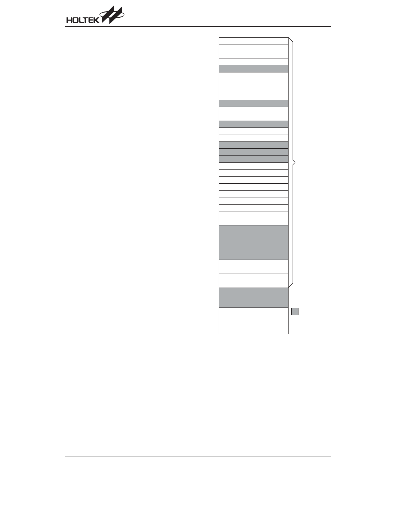
Data Memory - RAM
The data memory (RAM) is designed with 113´8 bits,
and is divided into two functional groups, namely; spe-
cial function registers (25´8 bits) and general purpose
data memory (88´8bit) most of which are read-
able/writable, although some are read only. Of the two
types of functional groups, the special function registers
consist of an Indirect addressing register 0 (00H), a
Memory pointer register 0 (MP0;01H), an Indirect ad-
dressing register 1 (02H), a Memory pointer register 1
(MP1;03H), an Accumulator (ACC;05H), a Program
counter lower-order byte register (PCL;06H), a Table
pointer (TBLP;07H), a Table higher-order byte register
00H
In d ir e c t A d d r e s s in g R e g is te r 0
01H
M P0
02H
In d ir e c t A d d r e s s in g R e g is te r 1
03H
M P1
04H
05H
ACC
06H
PCL
07H
TB LP
08H
TB LH
09H
0A H
STATU S
0B H
IN T C
0C H
0D H
TM R
0E H
TM R C
0FH
10H
11H
12H
PA
13H
PAC
14H
PB
15H
PBC
16H
PC
17H
PCC
18H
PD
19H
PDC
1A H
PW M
1B H
1C H
1D H
1E H
1FH
20H
ADRL
21H
ADRH
22H
ADCR
23H
ACSR
24H
S p e c ia l P u r p o s e
D ATA M EM O R Y
27H
28H
G e n e ra l P u rp o s e
:U nused
D a ta M e m o ry
R e a d a s "0 0 "
(8 8 B y te s )
7FH
RAM Mapping
(TBLH;08H), a Status register (STATUS;0AH), an Inter-
rupt control register (INTC;0BH), a Timer/Event Counter
(TMR:0DH), a Timer/Event Counter control register
(TMRC;0EH), PWM data register (PWM;1AH), the A/D
result lower-order byte register (ADRL;20H), the A/D re-
sult higher-order byte register (ADRH;21H), the A/D
control register (ADCR;22H), the A/D clock setting reg-
ister (ACSR;23H), I/O registers (PA;12H, PB;14H,
PC;16H, PD;18H), and I/O control registers (PAC;13H,
PBC;15H, PCC; 17H, PDC;19H). The remaining space
before the 28H is reserved for future expanded usage
and reading these locations will return the result ²00H².
The general purpose data memory, addressed from
Rev. 1.40
8
July 12, 2005
Share Link: 