HT46C24 Просмотр технического описания (PDF) - Holtek Semiconductor
Номер в каталоге
Компоненты Описание
производитель
HT46C24 Datasheet PDF : 51 Pages
| |||
HT46R24/HT46C24
value from the stack. After a chip reset, the SP will point
to the top of the stack.
If the stack is full and a non-masked interrupt takes
place, the interrupt request flag will be recorded but the
acknowledgment will be inhibited. When the stack
pointer is decremented (by RET or RETI), the interrupt is
serviced. This feature prevents stack overflow, allowing
the programmer to use the structure more easily. If the
stack is full and a ²CALL² is subsequently executed,
stack overflow occurs and the first entry will be lost (only
the most recent 16 return addresses are stored).
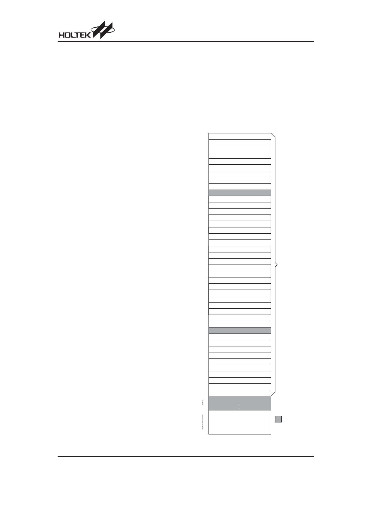
Data Memory - RAM
The data memory (RAM) is designed with 424´8 bits,
and is divided into two functional groups, namely; spe-
cial function registers (40´8 bits) and general purpose
data memory (Bank 0:192´8 bits and Bank 1:192´8
bits) most of which are readable/writeable, although
some are read only.
The special function registers are overlapped in any
banks. Of the two types of functional groups, the special
function registers consist of an Indirect addressing reg-
ister 0 (00H), a Memory pointer register 0 (MP0;01H),
an Indirect addressing register 1 (02H), a Memory
pointer register 1 (MP1;03H), a Bank pointer (BP;04H),
an Accumulator (ACC;05H), a Program counter
lower-order byte register (PCL;06H), a Table pointer
(TBLP;07H), a Table higher-order byte register
(TBLH;08H), a Status register (STATUS;0AH), an Inter-
rupt control register 0 (INTC0;0BH), a Timer/Event
Counter 0 (TMR0H:0CH; TMR0L:0DH), a Timer/Event
Counter 0 control register (TMR0C;0EH), a Timer/Event
Counter 1 (TMR1H:0FH; TMR1L:10H), a Timer/Event
Counter 1 control register (TMR1C; 11H), Interrupt con-
trol register 1 (INTC1;1EH), PWM data register
(PWM0;1AH, PWM1;1BH, PWM2;1CH, PWM3;1DH),
the I2C Bus slave address register (HADR;20H), the I2C
Bus control register (HCR;21H), the I2C Bus status reg-
ister (HSR;22H), the I2C Bus data register
(HDR;23H),the A/D result lower-order byte register
(ADRL;24H), the A/D result higher-order byte register
(ADRH;25H), the A/D control register (ADCR;26H), the
A/D clock setting register (ACSR;27H), I/O registers
(PA;12H, PB;14H, PC;16H, PD;18H, PF; 28H) and I/O
control registers (PAC;13H, PBC;15H, PCC;17H,
PDC;19H, PFC;29H). The remaining space before the
40H is reserved for future expanded usage and reading
these locations will get ²00H². The space before 40H is
overlapping in each bank. The general purpose data
memory, addressed from 40H to FFH (Bank0; BP=0 or
Bank1; BP=1), is used for data and control information
under instruction commands.
All of the data memory areas can handle arithmetic,
logic, increment, decrement and rotate operations di-
rectly. Except for some dedicated bits, each bit in the
data memory can be set and reset by ²SET [m].i² and
²CLR [m].i². They are also indirectly accessible through
memory pointer registers (MP0;01H/MP1;03H). The
space before 40H is overlapping in each bank.
After first setting up BP to the value of ²01H² to access
bank 1, this bank must then be accessed indirectly using
the Memory Pointer MP1. With BP set to a value of
²01H², using MP1 to indirectly read or write to the data
memory areas with addresses from 40H~FFH will result
in operations to bank 1. Directly addressing the Data
00H
In d ir e c t A d d r e s s in g R e g is te r 0
01H
M P0
02H
In d ir e c t A d d r e s s in g R e g is te r 1
03H
M P1
04H
BP
05H
ACC
06H
PCL
07H
TB LP
08H
TB LH
09H
0A H
STATU S
0B H
IN T C 0
0C H
TM R 0H
0D H
TM R 0L
0E H
TM R 0C
0FH
TM R 1H
10H
TM R 1L
11H
TM R 1C
12H
PA
13H
PAC
14H
PB
15H
PBC
16H
PC
17H
PCC
18H
PD
19H
PDC
1A H
PW M 0
1B H
PW M 1
1C H
PW M 2
1D H
PW M 3
1E H
IN T C 1
1FH
20H
HADR
21H
HCR
22H
HSR
23H
HDR
24H
ADRL
25H
ADRH
26H
ADCR
27H
ACSR
28H
PF
29H
PFC
30H
S p e c ia l P u r p o s e
D a ta M e m o ry
3FH
40H
G e n e ra l P u rp o s e
D a ta M e m o ry
:U nused
(1 9 2 B y te s ´ 2 B a n k : B a n k 0 ,B a n k 1 ) R e a d a s "0 0 "
FFH
RAM Mapping
Rev. 2.00
8
March 2, 2006
Share Link: 