HT46C24(2004) Просмотр технического описания (PDF) - Holtek Semiconductor
Номер в каталоге
Компоненты Описание
производитель
HT46C24 Datasheet PDF : 49 Pages
| |||
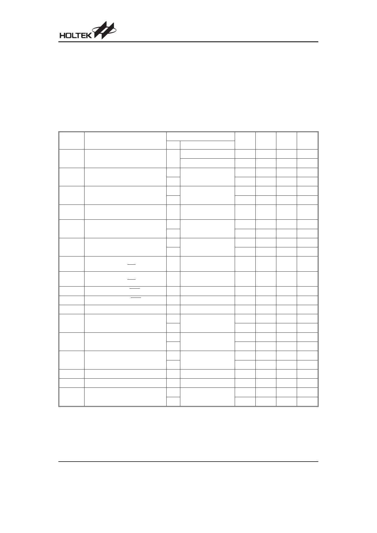
HT46R24/HT46C24
Pin Name
I/O
PC0~PC4
(28-pin package only)
I/O
PC0~PC7
(48-pin package only)
PD0/PWM0
PD1/PWM1/TMR1 I/O
(28-pin package only)
PD0/PWM0
PD1/PWM1
PD2/PWM2
PD3/PWM3
I/O
PD4~PD7
(48-pin package only)
PF0~PF7
I/O
(48-pin package only)
TMR0
I
TMR1
I
(48-pin package only)
RES
I
VSS
¾
VDD
¾
OSC1
I
OSC2
O
TEST1~3
I
NC
¾
Options
Pull-high
Pull-high
PWM
Pull-high
PWM
Pull-high
¾
¾
¾
¾
¾
Crystal
or RC
¾
¾
Description
Bidirectional 8-bit input/output port. Software instructions determine the
CMOS output, Schmitt trigger input with or without pull-high resistor (deter-
mine by pull-high option: byte option).
Bidirectional 8-bit input/output port. Software instructions determine the
CMOS output, Schmitt trigger input with or without a pull-high resistor.
The PWM0 output function is pin-shared with PD0.
The PWM1 output function is pin-shared with PD1 and TMR1.
(determined by pull-high option: byte option)
Bidirectional 8-bit input/output port. Software instructions determine the
CMOS output, Schmitt trigger input with or without a pull-high resistor (de-
termined by pull-high option: byte option). The PWM0/PWM1/PWM2/
PWM3 output function are pin-shared with PD0/PD1/PD2/PD3 (depending
on the PWM options).
Bidirectional 8-bit input/output port. Software instructions determine the
CMOS output, Schmitt trigger input with or without pull-high resistor (deter-
mine by pull-high option: byte option).
Timer/Event Counter 0 Schmitt trigger input (without pull-high resistor)
Timer/Event Counter 1 Schmitt trigger input (without pull-high resistor).
Schmitt trigger reset input, active low
Negative power supply, ground
Positive power supply
OSC1 and OSC2 are connected to an RC network or a crystal (by options)
for the internal system clock. In the case of RC operation, OSC2 is the
output terminal for 1/4 system clock.
Test mode input pin it disconnects in normal operation.
No connection
Absolute Maximum Ratings
Supply Voltage ...........................VSS-0.3V to VSS+6.0V
Input Voltage..............................VSS-0.3V to VDD+0.3V
Storage Temperature ............................-50°C to 125°C
Operating Temperature...........................-40°C to 85°C
Note: These are stress ratings only. Stresses exceeding the range specified under ²Absolute Maximum Ratings² may
cause substantial damage to the device. Functional operation of this device at other conditions beyond those
listed in the specification is not implied and prolonged exposure to extreme conditions may affect device reliabil-
ity.
D.C. Characteristics
Symbol
Parameter
VDD
Operating Voltage
IDD1
Operating Current (Crystal OSC)
IDD2
Operating Current (RC OSC)
Test Conditions
VDD
Conditions
fSYS=4MHz
¾
fSYS=8MHz
3V No load, fSYS=4MHz
5V ADC disable
3V No load, fSYS=4MHz
5V ADC disable
Ta=25°C
Min. Typ. Max. Unit
2.2
¾
5.5
V
3.3
¾
5.5
V
¾
0.6
1.5
mA
¾
2
4
mA
¾
0.8
1.5
mA
¾
2.5
4
mA
Rev. 1.50
4
May 3, 2004
Share Link: 