HT46R14 Просмотр технического описания (PDF) - Holtek Semiconductor
Номер в каталоге
Компоненты Описание
производитель
HT46R14 Datasheet PDF : 47 Pages
| |||
HT46R14
The A/D converter interrupt is initialized by setting the
A/D converter request flag (ADF; bit 6 of the INTC1), is
caused by an end of A/D conversion. When the interrupt
is enabled, the stack is not full and the ADF is set, a sub-
routine call to location 018H will occur. The related inter-
rupt request flag (ADF) will be reset and the EMI bit
cleared to disable further interrupts. After the interrupt is
enabled, and a subroutine call to location 018H occurs.
During the execution of an interrupt subroutine, other in-
terrupt acknowledgments are all held until the ²RETI² in-
struction is executed or the EMI bit and the related
interrupt control bit are set both to 1 (if the stack is not
full). To return from the interrupt subroutine, ²RET² or
²RETI² may be invoked. RETI sets the EMI bit and en-
ables an interrupt service, but RET does not.
Interrupts occurring in the interval between the rising
edges of two consecutive T2 pulses are serviced on the
latter of the two T2 pulses if the corresponding interrupts
are enabled. In the case of simultaneous requests, the
priorities in the following table apply. These can be
masked by resetting the EMI bit.
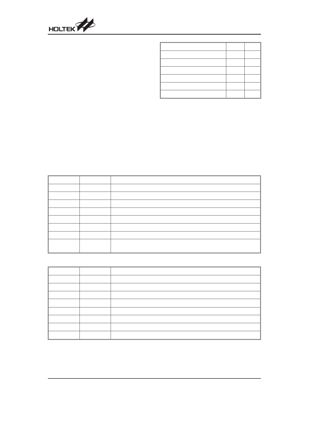
Interrupt Source
External interrupt 0
External interrupt 1
Comparator 0 output interrupt
Timer/Event Counter 0 overflow
Timer/Event Counter 1 overflow
A/D converter interrupt
Priority Vector
1
04H
2
08H
3
0CH
4
10H
5
14H
6
18H
The Comparator 0 interrupt request flag (C0F), external
interrupt 1 request flag (EI1F), External Interrupt 0 re-
quest flag (EI0F), Enable Comparator 0 output interrupt
bit (EC0I), Enable External interrupt 1 bit (EEI1), Enable
External Interrupt 0 bit (EEI0), and enable master inter-
rupt bit (EMI) make up of the Interrupt Control register 0
(INTC0) which is located at 0BH in the RAM.
Bit No.
0
1
2
3
4
5
6
7
Label
EMI
EEI0
EEI1
EC0I
EI0F
EI1F
C0F
¾
Function
Controls the master (global) interrupt (1=enable; 0=disable)
Controls the external interrupt 0 (1=enable; 0=disable)
Controls the external interrupt 1 (1=enable; 0=disable)
Control the Comparator 0 interrupt (1= enable; 0= disable)
External interrupt 0 request flag (1=active; 0=inactive)
External interrupt 1 request flag (1=active; 0=inactive)
The Comparator 0 request flag (1=active; 0=inactive)
For test mode used only.
Must be written as ²0²; otherwise may result in unpredictable operation.
INTC0 (0BH) Register
Bit No.
0
1
2
3
4
5
6
7
Label
ET0I
ET1I
EADI
¾
T0F
T1F
ADF
¾
Function
Controls the Timer/Event Counter 0 interrupt (1=enable; 0=disable)
Controls the Timer/Event Counter 1 interrupt (1=enable; 0=disable)
Controls the A/D converter interrupt (1=enable; 0=disable)
Unused bit, read as ²0²
Internal Timer/Event Counter 0 request flag (1=active; 0=inactive)
Internal Timer/Event Counter 1 request flag (1=active; 0=inactive)
The A/D converter request flag (1=active; 0=inactive)
Unused bit, read as ²0²
INTC1 (1EH) Register
Rev. 1.00
10
November 1, 2005
Share Link: 