HT46R12 Просмотр технического описания (PDF) - Holtek Semiconductor
Номер в каталоге
Компоненты Описание
производитель
HT46R12 Datasheet PDF : 45 Pages
| |||
HT46R12
Stack Register - STACK
This is a special part of the memory which is used to
save the contents of the program counter only. The
stack is organized into 8 levels and is neither part of the
data nor part of the program space, and is neither read-
able nor writeable. The activated level is indexed by the
stack pointer (SP) and is neither readable nor writeable.
At a subroutine call or interrupt acknowledge signal, the
contents of the program counter are pushed onto the
stack. At the end of a subroutine or an interrupt routine,
signaled by a return instruction (RET or RETI), the pro-
gram counter is restored to its previous value from the
stack. After a chip reset, the SP will point to the top of the
stack.
If the stack is full and a non-masked interrupt takes
place, the interrupt request flag will be recorded but the
acknowledge signal will be inhibited. When the stack
pointer is decremented (by RET or RETI), the interrupt
will be serviced. This feature prevents stack overflow al-
lowing the programmer to use the structure more easily.
In a similar case, if the stack is full and a ²CALL² is sub-
sequently executed, stack overflow occurs and the first
entry will be lost (only the most recent 8 return ad-
dresses are stored).
Data Memory - RAM
The data memory is organized into 115´8 bits, and is di-
vided into two functional groups, namely; special func-
tion registers and general purpose data memory (88´8
bits), most of which are readable/writeable, although
some are read only.
The special function registers consist of an Indirect ad-
dressing register 0 (00H), a Memory pointer register 0
(MP0;01H), an Indirect addressing register 1 (02H), a
Memory pointer register 1 (MP1;03H), an Accumulator
(;05H), a Program counter lower-order byte register
(PCL;06H), a Table pointer (TBLP;07H), a Table
higher-order byte register (TBLH;08H), a Status register
(STATUS;0AH), an Interrupt control register 0
(INTC0;0BH), a Timer/Event Counter 0 (TMR0;0DH), a
Timer/Event Counter 0 control register (TMR0C;0EH), a
Timer/Event Counter 1 (TMR1;10H), a Timer/Event
Counter 1 control register (TMR1C;11H), Interrupt con-
trol register 1 (INTC1;1EH), the A/D result lower-order
byte register (ADRL;24H), the A/D result higher-order
byte register (ADRH;25H), the A/D control register
(ADCR;26H), the A/D clock setting register
(ACSR;27H), I/O registers (PA;12H, PB;14H, PC;16H)
and I/O control registers (PAC;13H, PBC;15H,
PCC;17H), the programmable pulse generator (PPG)
control register (PPG0C;20H), and the programmable
pulse generator timer register (PPGT0;21H). The re-
maining space before the 28H is reserved for future
expansion usage and reading these locations will get a
²00H². The general purpose data memory, addressed
from 28H to 7FH is used for data and control information
under instruction commands.
All of the data memory areas can handle arithmetic,
logic, increment, decrement and rotate operations di-
rectly. Except for some dedicated bits, each bit in the
data memory can be set and reset by ²SET [m].i² and
²CLR [m].i². They are also indirectly accessible through
memory pointer register (MP0;01H/MP1;03H).
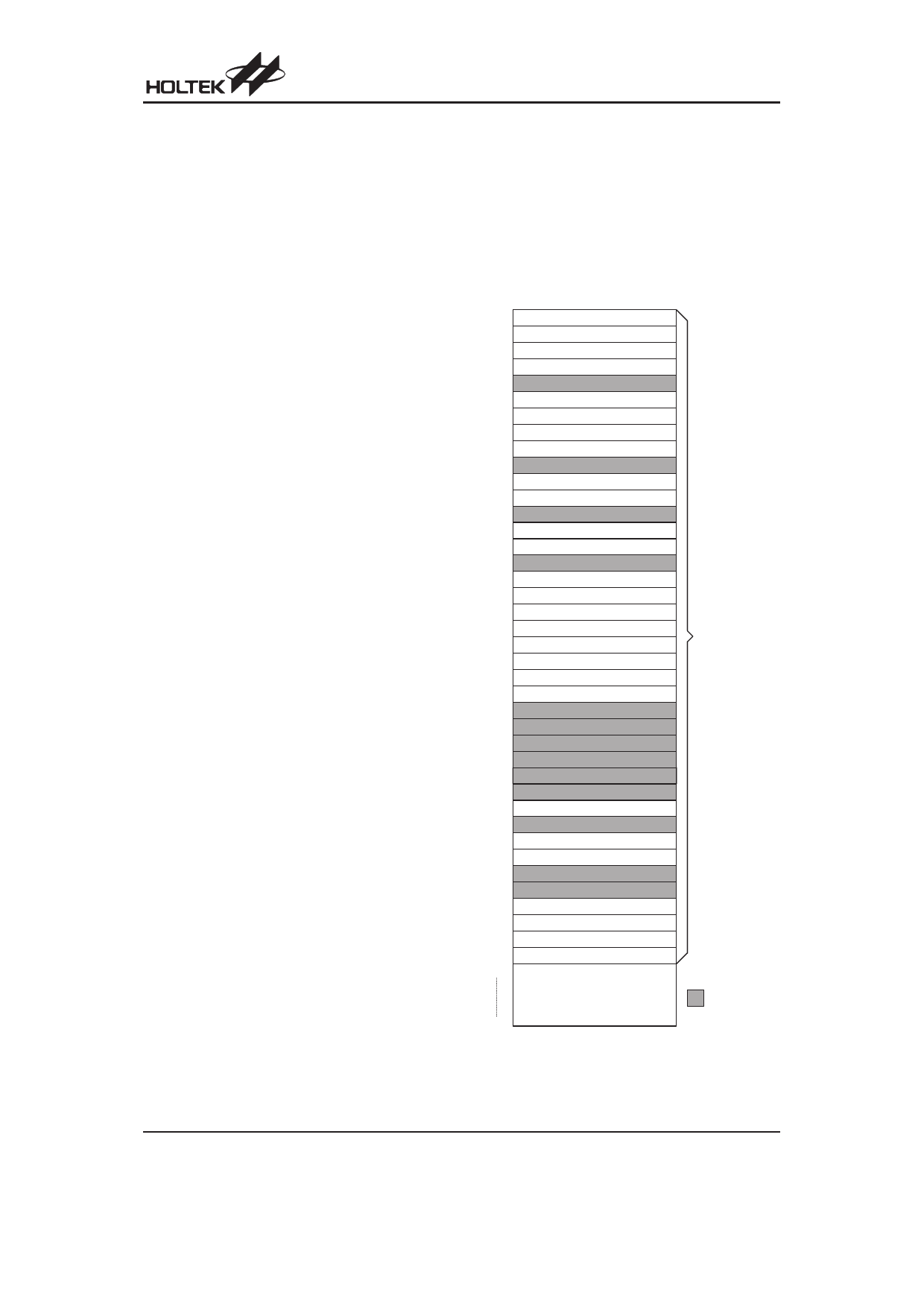
00H
In d ir e c t A d d r e s s in g R e g is te r 0
01H
M P0
02H
In d ir e c t A d d r e s s in g R e g is te r 1
03H
M P1
04H
05H
ACC
06H
PCL
07H
TB LP
08H
TB LH
09H
0A H
STATU S
0B H
IN T C 0
0C H
0D H
TM R 0
0E H
TM R 0C
0FH
10H
TM R 1
11H
TM R 1C
12H
PA
13H
PAC
14H
PB
S p e c ia l P u r p o s e
D a ta M e m o ry
15H
PBC
16H
PC
17H
PCC
18H
19H
1A H
1B H
1C H
1D H
1E H
IN T C 1
1FH
20H
P P G 0C
21H
PPG T0
22H
23H
24H
ADRL
25H
ADRH
26H
ADCR
27H
ACSR
28H
G e n e ra l P u rp o s e
D a ta M e m o ry
:U nused
(8 8 B y te s )
7FH
R e a d a s "0 0 "
RAM Mapping
Rev. 1.00
8
November 1, 2005
Share Link: 