HT16511 Просмотр технического описания (PDF) - Holtek Semiconductor
Номер в каталоге
Компоненты Описание
производитель
HT16511 Datasheet PDF : 12 Pages
| |||
HT16511
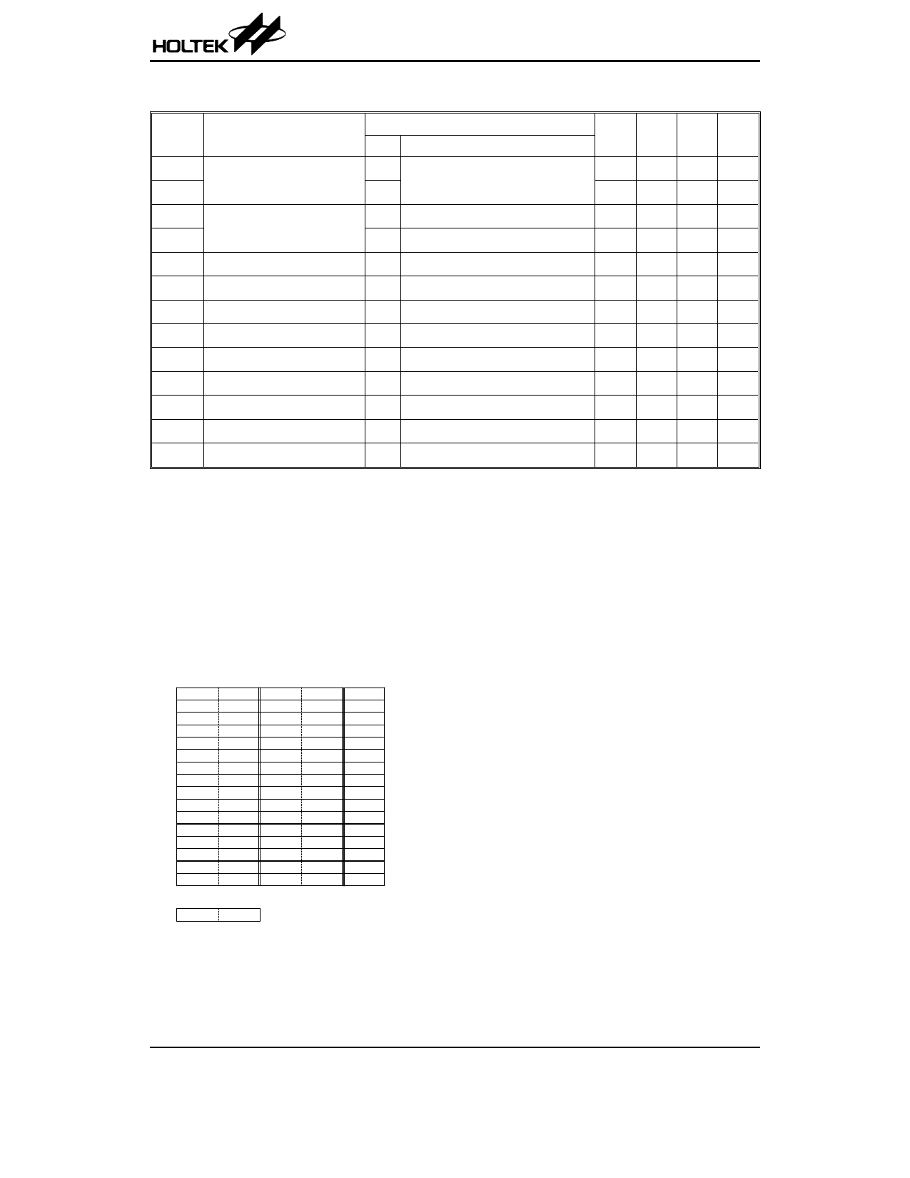
A.C. Characteristics
Symbol
Parameter
tPHL
Propagation Delay Time
tPLH
tr1
Rise Time
tr2
tf
Fall Time
tmax
Maximum Clock Frequency
Ci
Input Capacitance
tCW
Clock Pulse Width
tSW
Strobe Pulse Width
tSU
Data Setup Time
th
Data Hold Time
tCS
Clock-Strobe Time
tW
Wait Time
Test Conditions
VDD
Conditions
Min.
5V CLK®DO
¾
5V CL=15pF, RL=10kW
¾
5V CL=300pF, S0~S12
¾
5V CL=300pF, G1~G16
¾
5V CL=300pF, Sn, Gn
¾
5V Duty=50%
1
5V
¾
¾
5V
¾
400
5V
¾
1
5V
¾
100
5V
¾
100
5V CLK rising edge to CS rising edge 1
5V CLK rising edge to CLK falling edge 1
Ta=25°C
Typ. Max. Unit
¾ 300 ns
¾ 100 ns
¾
2
ms
¾ 0.5 ms
¾ 120 ms
¾ ¾ MHz
¾ 15 pF
¾ ¾ ns
¾ ¾ us
¾ ¾ ns
¾ ¾ ns
¾ ¾ ms
¾ ¾ ms
Functional Description
Display RAM and Display Mode
The static display RAM is organized into 40´8 bits and
stores the data transmitted from an external device to
the HT16511 through a serial interface. The contents of
the RAM are directly mapped to the contents of the VFD
driver. Data in the RAM can be accessed through the
data setting, address setting and display control com-
mands. It is assigned addresses in 8-bit unit as follows:
S E G 1 S E G 4 S E G 8 S E G 12 S E G 16 S E G 20
00H L
03H L
06H L
09H L
0C H L
0FH L
12H L
15H L
18H L
1B H L
1E H L
21H L
24H L
27H L
2A H L
2D H L
00H U
03H U
06H U
09H U
0C H U
0FH U
12H U
15H U
18H U
1B H U
1E H U
21H U
24H U
27H U
2A H U
2D H U
01H L
04H L
07H L
0A H L
0D H L
10H L
13H L
16H L
19H L
1C H L
1FH L
22H L
25H L
28H L
2B H L
2E H L
01H U
04H U
07H U
0A H U
0D H U
10H U
13H U
16H U
19H U
1C H U
1FH U
22H U
25H U
28H U
2B H U
2E H U
02H L
05H L
08H L
0B H L
0E H L
11H L
14H L
17H L
1A H L
1D H L
20H L
23H L
26H L
29H L
2C H L
2FH L
D IG 1
D IG 2
D IG 3
D IG 4
D IG 5
D IG 6
D IG 7
D IG 8
D IG 9
D IG 1 0
D IG 1 1
D IG 1 2
D IG 1 3
D IG 1 4
D IG 1 5
D IG 1 6
b0
b3b4
b7
XXHL XXHU
L o w e r H ig h e r
4 b its 4 b its
Note:
Only the lower 4 bits of the addresses assigned
to SEG17 through SEG20 are valid, the higher
4 bits are ignored.
Dimming Control
HT16511 provides 8-step dimmer function on display by
controlling the 3-bit binary command code. The full
pulse width of grid signal is divides into 16 uniform sec-
tions by PWM (pulse width modulation) technology.
The 16 uniform sections available form 8 steps dimmer
via 3-bit binary code. The 8-step dimmer includes 1/16,
2/16, 4/16, 10/16, 11/16, 12/16, 13/16 and 14/16. The
1/16 pulse width indicates minimum lightness. The
14/16 pulse width represents maximum lightness (Refer
to the display control command).
Key Matrix and Key-Input Data Storage RAM
The key matrix scans the series key states at each level
of the key strobe signal (S1/K1~S12/K12) output of the
HT16511. The key strobe signal outputs are
time-multiplexed signals from S1/K1~S12/K12. The
states of inputs K0~K3 are sampled by strobe signal
S1/K1~S12/K12 and latched into the register.
Rev. 1.10
5
September 18, 2003
Share Link: 