HSP43881 Просмотр технического описания (PDF) - Intersil
Номер в каталоге
Компоненты Описание
производитель
HSP43881 Datasheet PDF : 21 Pages
| |||
HSP43881
01
67
RESET.D
26
26 26
26
3
ADR0.D-ADR2.D
CELL RESULT
MUX
0-18
18
SIGN EXT
18-25
8
26
18 (LSBs)
0-17
+
SHADD
CLR SHADD.D
D
Q
ZERO
MUX
01
CLK
18
8-25
26
OUTPUT
BUFFER
26
RESET.D
CLK
18 MSBs SHIFTED
8 BITS TO RIGHT
(BITS 0 - 17)
0
RESET.D
CLR
D
Q
26
10
OUTPUT
MUX
26
SENBL 2 THREE-STATE
SENBH
BUFFER
CLK
26
SUM0-25
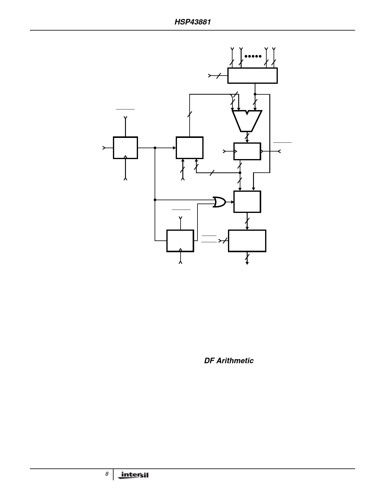
FIGURE 2. DF OUTPUT STAGE
The 26 least significant bits (LSBs) from either a cell
accumulator or the output buffer are output on the SUM0-25
bus. The output mux determines whether the cell
accumulator selected by ADR0-2 or the output buffer is
output to the bus. This mux is controlled by the SHADD input
signal. Control is based on the state of the SHADD during
two successive clocks; in other words, the output mux
selection contains memory. If SHADD is low during a clock
cycle and was low during the previous clock, the output mux
selects the contents of the filter cell accumulator addressed
by ADR0-2. Otherwise the output mux selects the contents
of the output buffer.
If the ADR0-2 lines remain at the same address for more
than one clock, the output at SUM0-25 will not change to
reflect any subsequent accumulator updates in the
addressed cell. Only the result available during the first clock
when ADR0-2 selects the cell will be output. This does not
hinder normal FIR operation since the ADR0-2 lines are
changed sequentially. This feature facilitates the interface
with slow memories where the output is required to be fixed
for more than one clock.
8
The SUM0-25 output bus is controlled by the SENBH and
SENBL signals. A low on SENBL enables bits SUM0-15. A
low on SENBH enables bits SUM16-25. Thus, all 26 bits can
be output simultaneously if the external system has a 26-bit
or larger bus. If the external system bus is only 16 bits, the
bits can be enabled in two groups of 16 and 10 bits (sign
extended).
DF Arithmetic
Both data samples and coefficients can be represented as
either unsigned or two's complement numbers. The TCS and
TCCI inputs determine the type of arithmetic representation.
Internally all values are represented by a 9-bit two's
complement number. The value of the additional ninth bit
depends on the arithmetic representation selected. For two's
complement arithmetic, the sign is extended into the ninth
bit. For unsigned arithmetic, bit-9 is 0.
The multiplier output is 18 bits and the accumulator is 26
bits. The accumulator width determines the maximum
possible number of terms in the sum of products without
Share Link: 