HIP0060AB Просмотр технического описания (PDF) - Intersil
Номер в каталоге
Компоненты Описание
производитель
HIP0060AB Datasheet PDF : 7 Pages
| |||
HIP0060
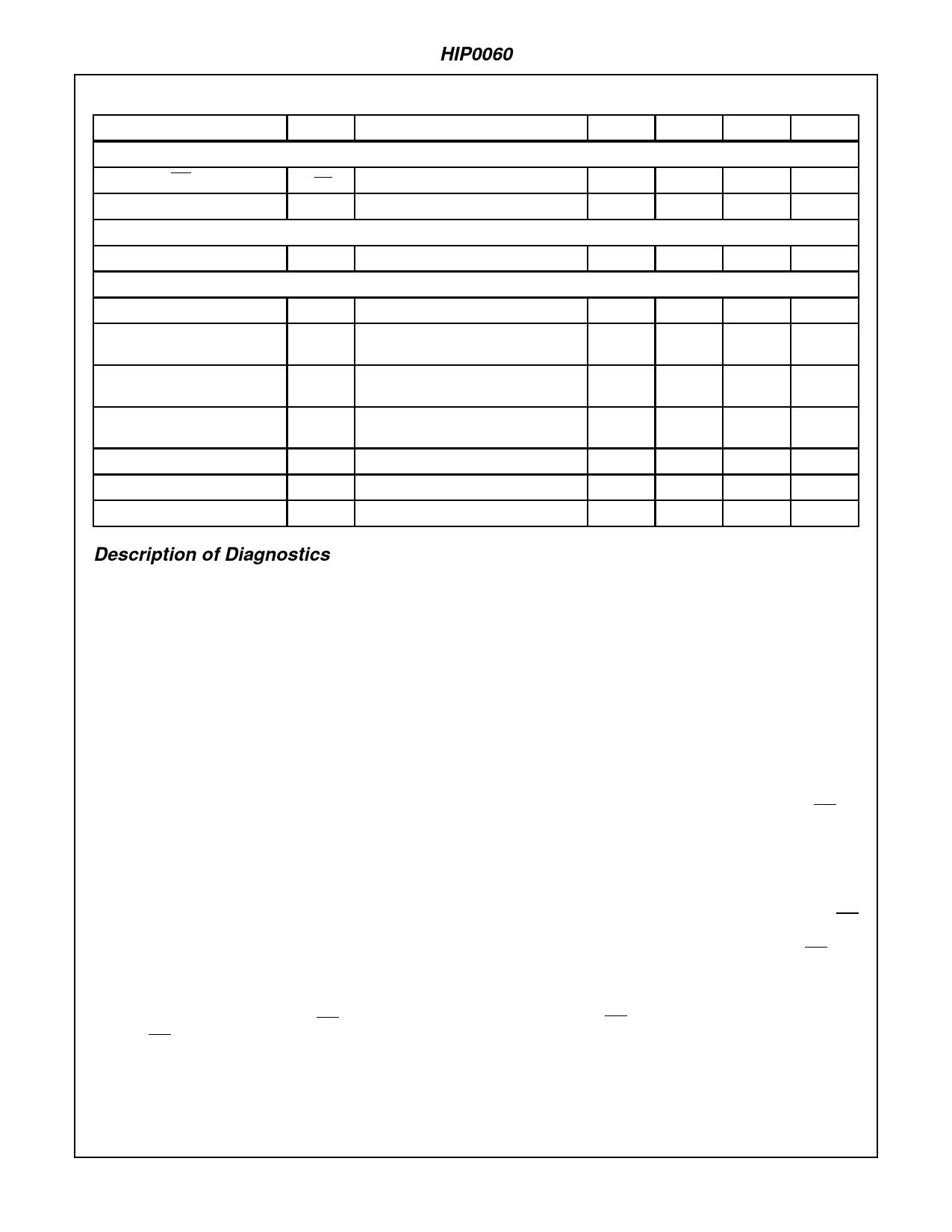
Electrical Specifications VDD = 4.5V to 5.5V, VSS = 0V, TA = -40oC to 125oC; Unless Otherwise Specified (Continued)
PARAMETER
SYMBOL
CONDITIONS
MIN
TYP
MAX
UNITS
DIAGNOSTIC
Pulse Width, INT
t INT
3
-
25
µs
Fault Response Time
tFAULT
-
-
16
µs
OVER-TEMPERATURE PROTECTION
Over-Temperature Shutdown
TSD
160
-
-
oC
SERIAL PERIPHERAL INTERFACE TIMING (Capacitance Each Pin, CL = 200pF)
SCK Period
tCYC
500
-
-
ns
SCK Clock High/Low Time
tWSCKH,
tWSCKL
200
-
-
ns
SCK Rise/Fall Time
trSCK,
tfSCK
-
-
30
ns
Enable Lead/Lag Time
tLEAD,
tLAG
250
-
-
ns
Output Data Valid Time
tV
-
-
170
ns
Data Setup Time
tSU
-
-
30
ns
Disable Time
tDIS
-
-
250
ns
Description of Diagnostics
OC (Over-Current) Fault Mode
In a short circuit or over-current fault condition when an out-
put is switched on, the output current is limited to the ICL
maximum as defined in the Electrical Specifications. An OC
fault condition does not shutdown the output. The current is
sensed and feedback is directed to the gate of the MOS Out-
put Driver. The gate voltage is reduced to maintained the
specified level of current limiting. In this mode, the drain volt-
age will increase and cause increased dissipation.
OT (Over-Temperature) Fault Mode
Under a high dissipation over-temperature fault condition,
the output temperature is detected and compared to a preset
threshold level. When the OT threshold is exceeded, thermal
shutdown for that output occurs. The Gate Control Latch
drive to the output is switched off and a status flag (the OT
Bit) for the fault is set. The output shutdown action is inde-
pendent of the IN input state. However, the Gate Control
Latch and OL Bit will be reset on the next rising edge of the IN
input and, if the fault still exists, the shutdown action will repeat.
Diagnostic action for an OT fault includes feedback of the
fault status to the Serial Diagnostic Register for a SPI bus
data output. Also, as shown in the Block Diagram, the OT
fault status bit information is ORed into a one-shot that
drives an open drain to provide an INT interrupt signal out-
put. The INT output has a specified timing from the one-shot
multi and is defined in the Electrical Specifications as tINT.
OL (Open-Load) Fault Mode
An open-load fault mode sequence consists of setting a sta-
tus flag (the OL Bit) when an output open load condition is
detected. If the output impedance is greater than a preset
threshold, as detected when the input is off; the status bit is
set. The OL Bit is reset on the next falling edge of the IN
input signal. The off-on detection sequence will repeat as
long as the output impedance is higher than the detection
threshold, as detected in the off state.
Diagnostic action for an OL fault mode differs from the OT
fault mode by not forcing an output shutdown through the
Gate Controlled Latch. Also, because the OL fault is
detected in the off state, the status flag is reset on the falling
edge of the input instead of the rising edge. The OL output
information to the Serial Diagnostic Register and the INT pin
is the same as the OT fault mode action.
ORed Fault Bits
It is important to note that the trigger input to the one-shot is
locked-out for the tINT duration and any fault that may have
occurred in the tINT window will not be displayed at the INT
output. However, all 8 fault bits may still be read as data from
the SO output when clock by the SCK input. The INT fault
output is provided as an interrupt signal to flag the immedi-
ate occurrence of a fault and take appropriate action as
defined by the microcontroller to the SPI bus and the users
programming. The INT fault output may be ORed with other
ICs to provide a system microcontroller interrupt to indicate
the presence of a fault.
3
Share Link: 