HD404848 Просмотр технического описания (PDF) - Hitachi -> Renesas Electronics
Номер в каталоге
Компоненты Описание
производитель
HD404848 Datasheet PDF : 125 Pages
| |||
HD404849 Series
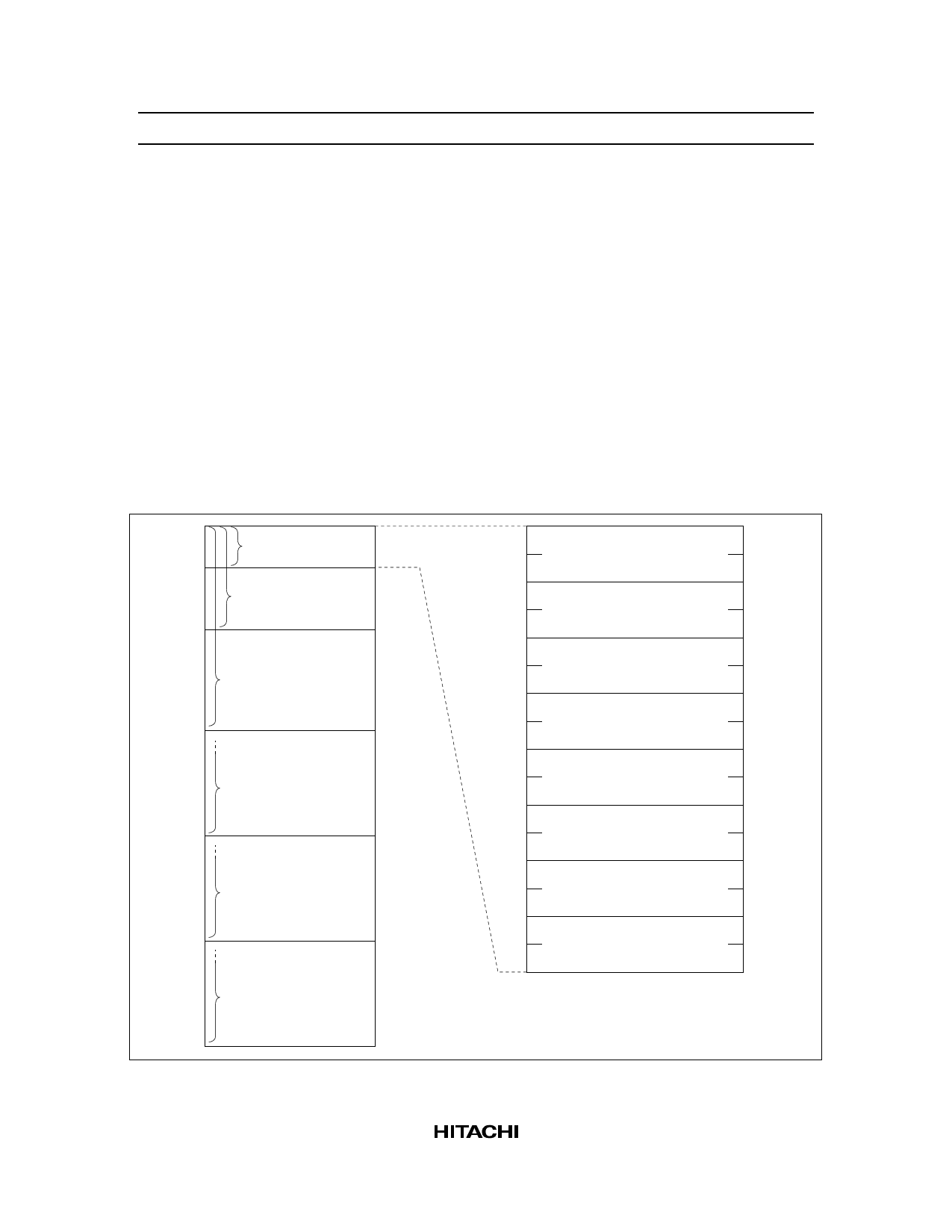
Memory Map
ROM Memory Map
The ROM memory map is shown in figure 1 and described below.
Vector Address Area ($0000–$000F): Reserved for JMPL instructions that branch to the start addresses
of the reset and interrupt routines. After MCU reset or an interrupt, program execution continues from the
vector address.
Zero-Page Subroutine Area ($0000–$003F): Reserved for subroutines. The program branches to a
subroutine in this area in response to the CAL instruction.
Pattern Area ($0000–$0FFF): Contains ROM data that can be referenced with the P instruction.
Program Area ($0000–$1FFF: HD404848; $0000–$2FFF: HD4048412; $0000–$3FFF: HD404849,
HD4074849): Used for program coding.
0
Vector address area $0000
15
(16 words)
$000F
Zero-page
subroutine area
(64 words)
63
$003F
Pattern area
(4,096 words)
4095
$0FFF
8191
HD404848
program area
(8,192 words)
$1FFF
12287
HD4048412
program area
(12,288 words)
16383
HD404849/
HD4074849
program area
(16,384 words)
$2FFF
$3FFF
0
JMPL instruction
$0000
1 (jump to RESET, STOPC routine) $0001
2
JMPL instruction
$0002
3
(jump to INT0 routine)
$0003
4
JMPL instruction
$0004
5
(jump to INT1 routine)
$0005
6
JMPL instruction
$0006
7
(jump to timer A routine)
$0007
8
JMPL instruction
$0008
9 (jump to timer B, INT2 routine) $0009
10
JMPL instruction
$000A
11 (jump to timer C, INT3 routine) $000B
12
JMPL instruction
$000C
13
(jump to timer D routine)
$000D
14
JMPL instruction
$000E
15
(jump to A/D, serial routine)
$000F
Figure 1 ROM Memory Map
7
Share Link: 