HAL11X Просмотр технического описания (PDF) - Micronas
Номер в каталоге
Компоненты Описание
производитель
HAL11X Datasheet PDF : 17 Pages
| |||
HAL11x
1.4. Operating Junction Temperature Range
The Hall sensors from Micronas are specified to the chip
temperature (junction temperature TJ).
K: TJ = –40 °C to +140 °C
E: TJ = –40 °C to +100 °C
C: TJ = 0 °C to +100 °C
The relationship between ambient temperature (TA) and
junction temperature is explained in section 5.2. on page
14.
1.5. Hall Sensor Package Codes
HAL XXXPA-T
Temperature Range: K, E, or C
Package: SF for SOT-89B
UA for TO-92UA
(SO for SOT-89A)
Type: 11x
Example: HAL114UA-E
→ Type: 114
→ Package: TO-92UA
→ Temperature Range: TJ = –40 °C to +100 °C
Hall sensors are available in a wide variety of packaging
versions and quantities. For more detailed information,
please refer to the brochure: “Ordering Codes for Hall
Sensors”.
1.6. Solderability
all packages: according to IEC68-2-58
During soldering reflow processing and manual
reworking, a component body temperature of 260 °C
should not be exceeded.
Components stored in the original packaging should
provide a shelf life of at least 12 months, starting from the
date code printed on the labels, even in environments as
extreme as 40 °C and 90% relative humidity.
1VDD
OUT
3
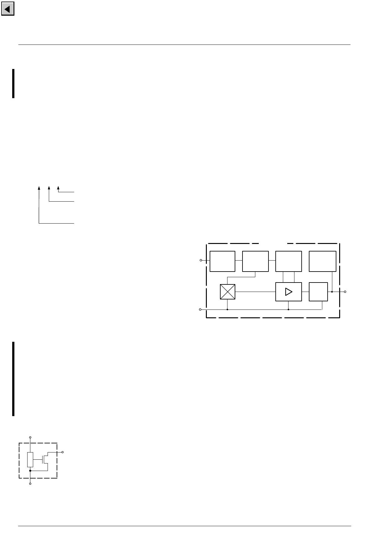
2. Functional Description
The HAL 11x sensors are monolithic integrated circuits
which switch in response to magnetic fields. If a
magnetic field with flux lines perpendicular to the
sensitive area is applied to the sensor, the biased Hall
plate forces a Hall voltage proportional to this field. The
Hall voltage is compared with the actual threshold level
in the comparator. The temperature-dependent bias
increases the supply voltage of the Hall plates and
adjusts the switching points to the decreasing induction
of magnets at higher temperatures. If the magnetic field
exceeds the threshold levels, the open drain output
switches to the appropriate state. The built-in hysteresis
eliminates oscillation and provides switching behavior of
output without bouncing.
Shunt protection devices clamp voltage peaks at the
Output-pin and VDD-pin together with external series
resistors. Reverse current is limited at the VDD-pin by an
internal series resistor up to –15 V. No external reverse
protection diode is needed at the VDD-pin for reverse
voltages ranging from 0 V to –15 V.
VDD
1
Reverse
Voltage &
Overvoltage
Protection
HAL 11x
Temperature
Dependent
Bias
Hysteresis
Control
Short Circuit &
Overvoltage
Protection
GND
2
Hall Plate
Comparator
Output
OUT
3
Fig. 2–1: HAL11x block diagram
2
GND
Fig. 1–1: Pin configuration
4
Micronas
Share Link: 