HA-5330 Просмотр технического описания (PDF) - Intersil
Номер в каталоге
Компоненты Описание
производитель
HA-5330 Datasheet PDF : 5 Pages
| |||
HA-5330
Absolute Maximum Ratings
Thermal Information
Voltage between V+ and SUPPLY/SIG GND . . . . . . . . . . . . . . +20V
Voltage between V- and SUPPLY/SIG GND . . . . . . . . . . . . . . . -20V
Voltage between SUPPLY GND and SIG GND . . . . . . . . . . . . ±2.0V
Voltage between S/H Control and SUPPLY/SIG GND . . . . +8V, -6V
Differential Input Voltage . . . . . . . . . . . . . . . . . . . . . . . . . . . . . . 24V
Output Current, Continuous (Note 1) . . . . . . . . . . . . . . . . . . . ±17mA
Operating Conditions
Thermal Resistance (Typical, Note 3)
θJA (oC/W) θJC (oC/W)
CERDIP Package. . . . . . . . . . . . . . . . .
66
16
PDIP Package . . . . . . . . . . . . . . . . . . .
90
N/A
Maximum Junction Temperature (Ceramic Package, Note 2) . . .175oC
Maximum Junction Temperature (Plastic Package) . . . . . . . .150oC
Maximum Storage Temperature Range . . . . . . . . . . -65oC to 150oC
Maximum Lead Temperature (Soldering 10s) . . . . . . . . . . . . 300oC
Temperature Range
HA-5330-2 . . . . . . . . . . . . . . . . . . . . . . . . . . . . . . -55oC to 125oC
HA-5330-5 . . . . . . . . . . . . . . . . . . . . . . . . . . . . . . . . 0oC to 75oC
Supply Voltage Range (Typical) . . . . . . . . . . . . . . . . . ±10V to ±20V
CAUTION: Stresses above those listed in “Absolute Maximum Ratings” may cause permanent damage to the device. This is a stress only rating and operation of the
device at these or any other conditions above those indicated in the operational sections of this specification is not implied.
NOTES:
1. Internal Power Dissipation may limit Output Current below ±17mA.
2. Maximum power dissipation, including output load, must be designed to maintain the junction temperature below 175oC for the ceramic package,
and below 150oC for the plastic package.
3. θJA is measured with the component mounted on an evaluation PC board in free air.
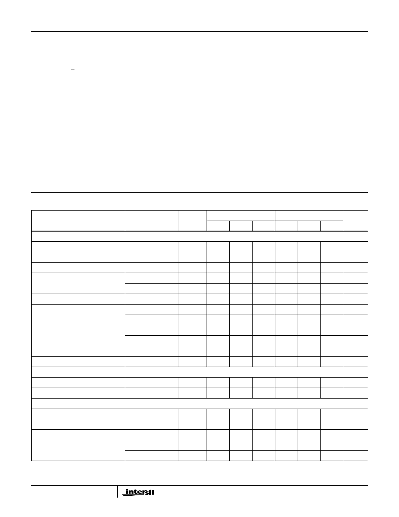
Electrical Specifications VSUPPLY = ±15V; S/H Control VIL = +0.8V (Sample): VIH = +2.0V (Hold); SIG GND = SUPPLY GND,
Unity Gain Configuration (Output tied to -Input), Unless Otherwise Specified
PARAMETER
TEST
CONDITIONS
TEMP.
(oC)
HA-5330-2
MIN TYP MAX
HA-5330-5
MIN TYP MAX
UNITS
INPUT CHARACTERISTICS
Input Voltage Range
Full
±10
-
-
±10
-
-
V
Input Resistance (Note 4)
25
5
15
-
5
15
-
MΩ
Input Capacitance
25
-
3
-
-
3
-
pF
Offset Voltage
25
-
0.2
-
-
0.2
-
mV
Offset Voltage Temperature Coefficient
Full
-
-
2.0
-
-
1.5
mV
Full
-
1
10
-
1
10
µV/oC
Bias Current
25
-
±20
-
-
±20
-
nA
Full
-
-
±500
-
-
±300
nA
Offset Current
25
-
20
-
-
20
-
nA
Full
-
-
500
-
-
300
nA
Common Mode Range
Full
±10
-
-
±10
-
-
V
CMRR
TRANSFER CHARACTERISTICS
Gain
VCM = ±10V
DC
Full
86
100
-
86
100
-
dB
Full
2 x 10⁶ 2 x 10⁷
-
2 x 10⁶ 2 x 10⁷
-
V/V
Gain Bandwidth Product
Note 12
25
-
4.5
-
-
4.5
-
MHz
OUTPUT CHARACTERISTICS
Output Voltage
Full
±10
-
-
±10
-
-
V
Output Current
Full
±10
-
-
±10
-
-
mA
Full Power Bandwidth (Note 6)
25
-
1.4
-
-
1.4
-
MHz
Output Resistance
Hold Mode
Sample Mode
25
-
0.2
-
-
0.2
-
Ω
25
-
10-5 0.001
-
10-5 0.001
Ω
2
Share Link: 