H7P1002DL Просмотр технического описания (PDF) - Renesas Electronics
Номер в каталоге
Компоненты Описание
производитель
H7P1002DL Datasheet PDF : 9 Pages
| |||
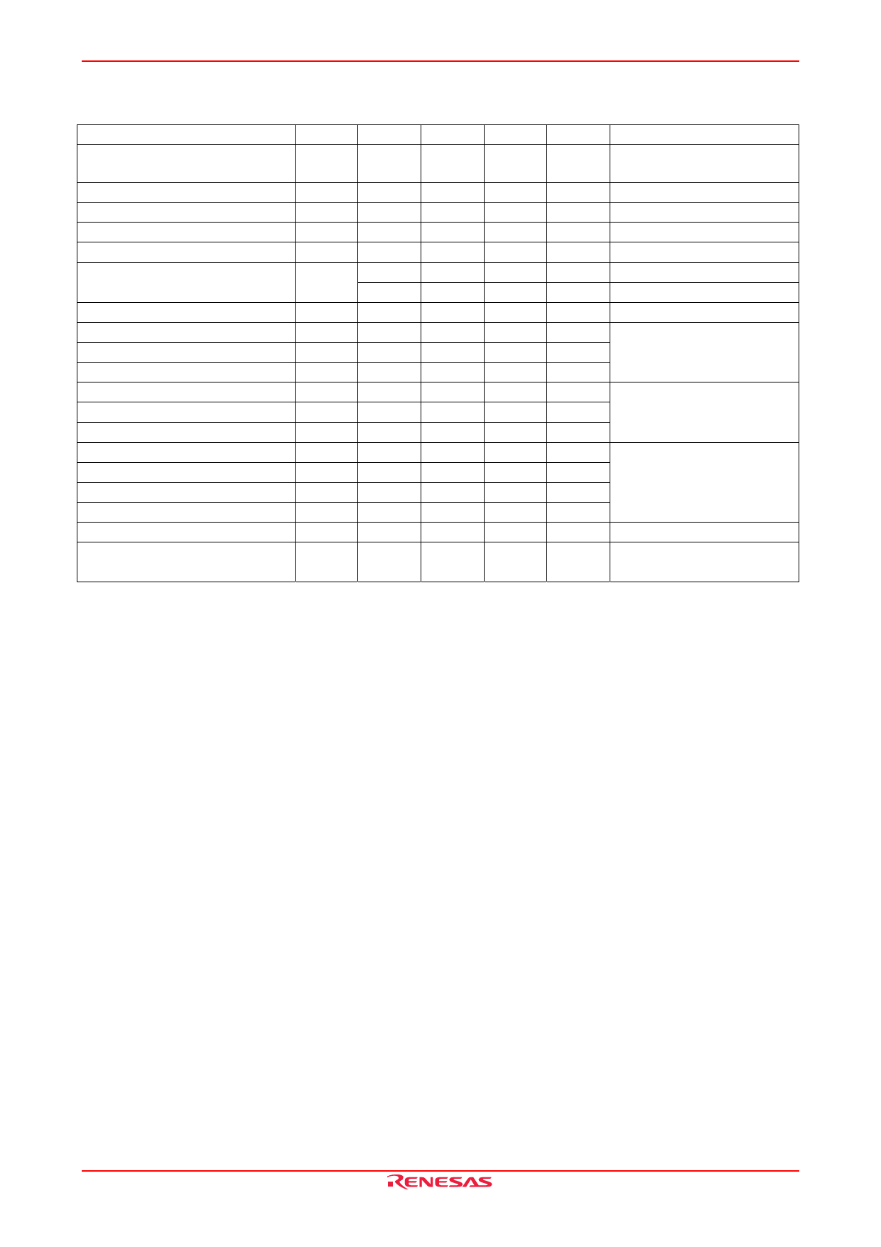
H7P1002DL, H7P1002DS
Electrical Characteristics
Item
Drain to source breakdown
voltage
Gate to source breakdown voltage
Gate to source leak current
Zero gate voltage drain current
Gate to source cutoff voltage
Static drain to source on state
resistance
Forward transfer admittance
Input capacitance
Output capacitance
Reverse transfer capacitance
Total gate charge
Gate to source charge
Gate to drain charge
Turn-on delay time
Rise time
Turn-off delay time
Fall time
Body-drain diode forward voltage
Body-drain diode reverse recovery
time
Note: 4. Pulse test
Symbol
V(BR)DSS
V(BR)GSS
IGSS
IDSS
VGS(off)
RDS(on)
|yfs|
Ciss
Coss
Crss
Qg
Qgs
Qgd
td(on)
tr
td(off)
tf
VDF
trr
Min
–100
±20
—
—
–1.0
—
—
7.2
—
—
—
—
—
—
—
—
—
—
—
—
Typ
—
—
—
—
—
85
105
12
2600
190
120
45
6.5
9.0
23
45
80
13
–0.91
50
Max
—
—
±10
–10
–2.5
105
150
—
—
—
—
—
—
—
—
—
—
—
—
—
(Ta = 25°C)
Unit
Test Conditions
V
ID = –10 mA, VGS = 0
V
IG = ±100 µA, VDS = 0
µA
VGS = ±16 V, VDS = 0
µA VDS = –100 V, VGS = 0
V
ID = –1 mA, VDS = –10 V Note4
mΩ
ID = –7.5 A, VGS = –10 V Note4
mΩ
ID = –7.5 A, VGS = –4.5 V Note4
S
ID = –7.5 A, VDS = –10 V Note4
pF VDS = –10 V
pF
VGS = 0
pF f = 1 MHz
nC VDD = –50 V
nC VGS = –10 V
nC ID = –15 A
ns VGS = –10 V, ID = –7.5 A
ns RL = 4.0 Ω
ns Rg = 4.7 Ω
ns
V
IF = –15 A, VGS = 0
ns
IF = –15 A, VGS = 0
diF/dt = 100 A/µs
REJ03G1601-0100 Rev.1.00 Nov 16, 2007
Page 2 of 8
Share Link: 