AZ100E111FNR2 Просмотр технического описания (PDF) - AZ Microtek
Номер в каталоге
Компоненты Описание
производитель
AZ100E111FNR2 Datasheet PDF : 6 Pages
| |||
AZ10E111
AZ100E111
AC Characteristics (VEE =10E(-4.94V to -5.46V), 100E(-4.2V to -5.46V); VCC =VCCO =GND or VEE =GND;
VCC =VCCO = 10E(+4.94V to +5.46V), 100E(+4.2V to +5.46V) )
Symbol
Characteristic
-40°C
0°C
25°C
85°C
Unit
Min Typ Max Min Typ Max Min Typ Max Min Typ Max
Propagation Delay
tPLH / tPHL to Output
IN (Diff)1 380
IN (SE)2
280
Enable3
400
Disable3
400
680 460
780 410
900 450
900 450
560 480
610 430
850 450
850 450
580 510
630 460
850 450
850 450
610
660 ps
850
850
tS
Setup Time E¯N¯ to IN5 250
0
200
0
200
0
200
0
ps
tH
Hold Time IN to E¯N¯ 6
50 -200
0 -200
0 -200
0 -200
ps
tR
Release Time E¯N¯ to IN7
350 100
300 100
300 100
300 100
ps
tSKEW
Within-Device Skew4
25
75
25
50
25
50
25
50
ps
VPP (AC) Minimum Input Swing8
250
250
250
250
mV
VCMR
Common Mode Range9
VCC -
1.6
VCC - VCC -
0.4 1.6
VCC - VCC -
0.4 1.6
VCC - VCC -
0.4 1.6
VCC -
0.4
V
tr / tf
Rise/Fall Time
250
650 275
600 275
600 275
600 ps
1. The differential propagation delay is defined as the delay from the crossing points of the differential input signals to the crossing point of the
differential output signals.
2. The single-ended propagation delay is defined as the delay from the 50% point of the input signal to the 50% point of the output signal.
3. Enable is defined as the propagation delay from the 50% point of a negative transition on E¯N¯ to the 50% point of a positive transition on Q (or a
negative transition on Q¯ ). Disable is defined as the propagation delay from the 50% point of a positive transition on E¯N¯ to the 50% point of a
negative transition on Q (or a positive transition on Q¯ ).
4. The within-device skew is defined as the worst-case difference between any two similar delay paths within a single device.
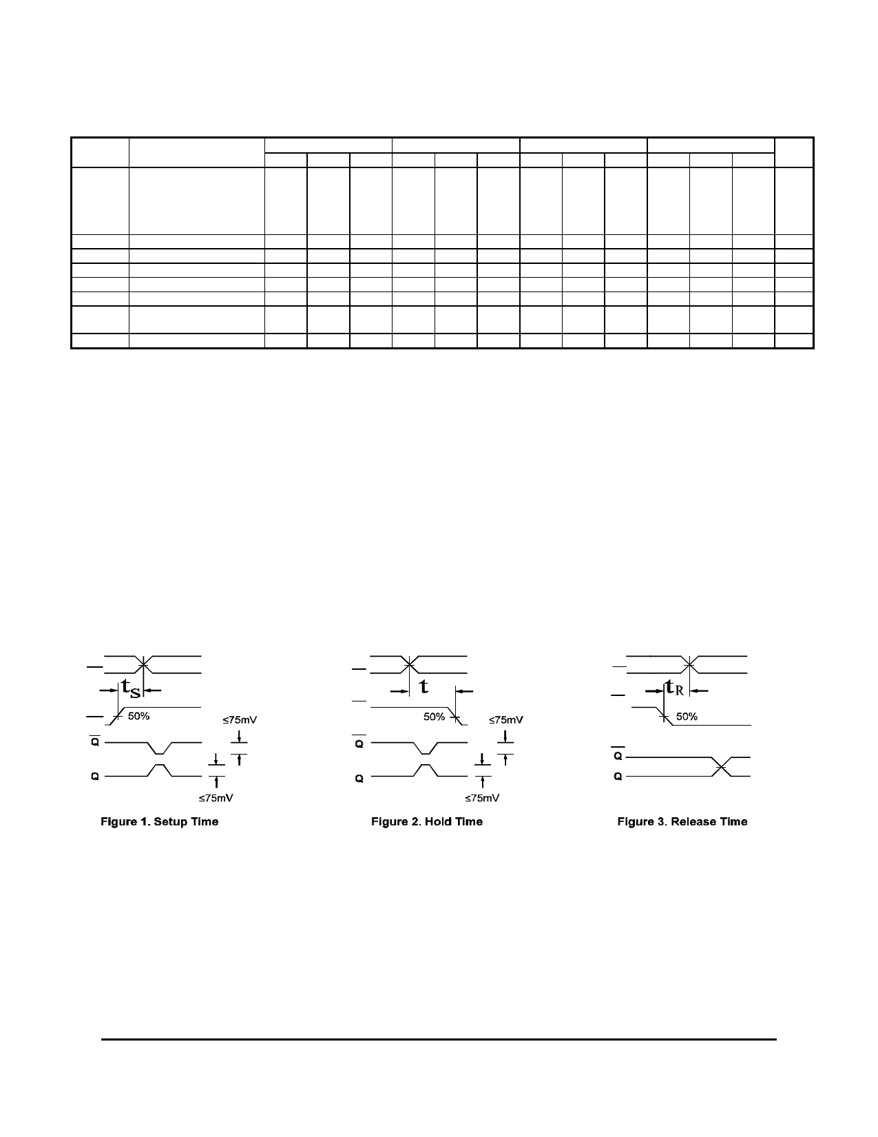
5. The setup time is the minimum time that E¯N¯ must be asserted prior to the next transition of IN/ I¯N¯ to prevent an output response greater than
±75mV to that IN/ I¯N¯ transition (see Figure 1).
6. The hold time is the minimum time that E¯N¯ must remain asserted after a negative going IN or a positive going I¯N¯ to prevent an output response
greater than ±75 mV to that IN/ I¯N¯ transition (see Figure 2).
7. The release time is the minimum time that E¯N¯ must be de-asserted prior to the next IN/ I¯N¯ transition to ensure an output response that meets the
specified IN to Q propagation delay and output transition times (see Figure 3).
8. VPP(min) is defined as the minimum peak-to-peak input differential voltage which will cause no increase in the propagation delay. The VPP(min)
is AC limited for the E111, because differential input as low as 50 mV will still produce full ECL levels at the output.
9. VCMR is defined as the range within which the VIH level may vary, with the device still meeting the propagation delay specification. The VIL level
must be such that the peak-to-peak voltage is less than 1.0V and greater than or equal to VPP(min).
IN
IN
IN
IN
IN
IN
H
EN
EN
EN
November 2006 * REV - 3
www.azmicrotek.com
4
Share Link: 