FXL2SD106 Просмотр технического описания (PDF) - Fairchild Semiconductor
Номер в каталоге
Компоненты Описание
производитель
FXL2SD106 Datasheet PDF : 14 Pages
| |||
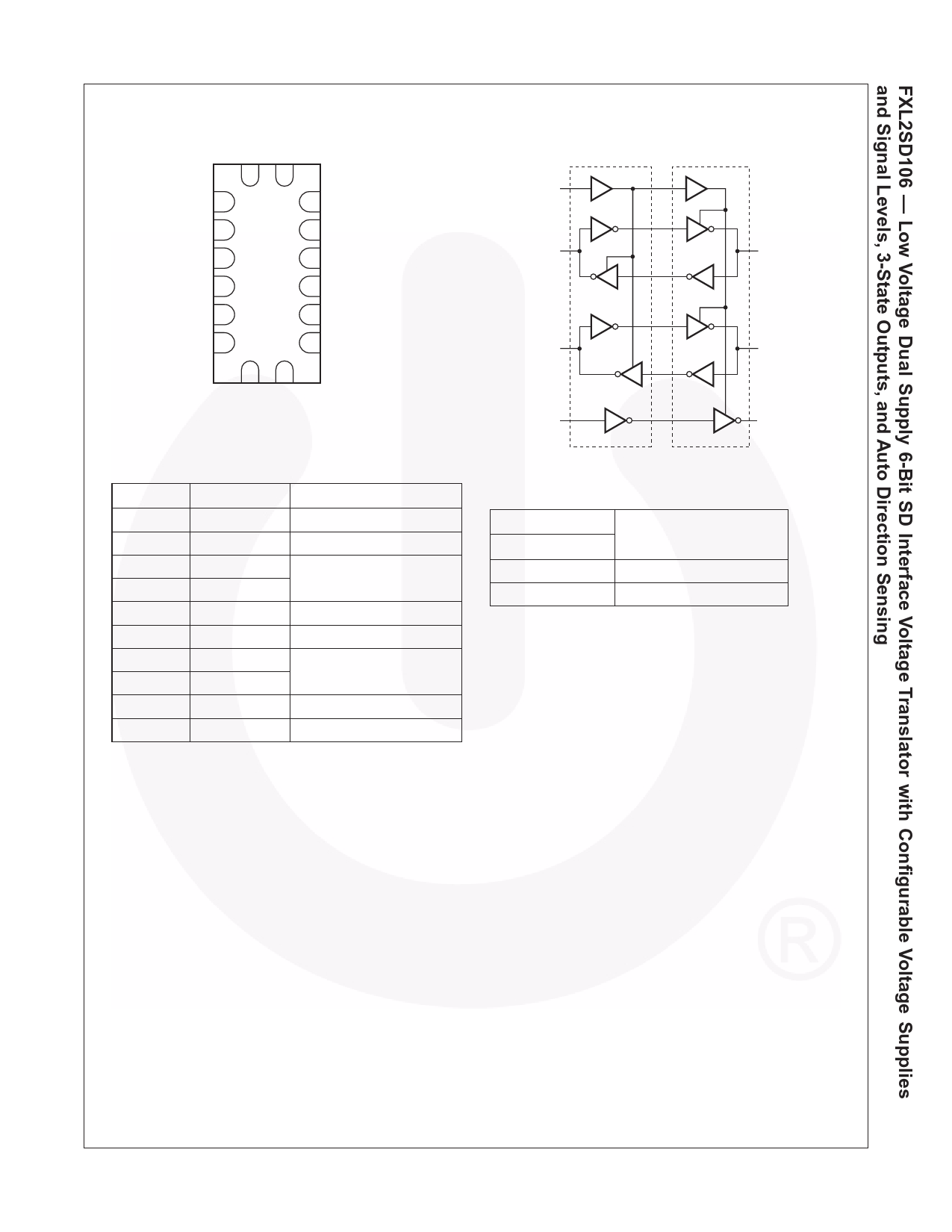
Connection Diagram
VCCA VCCB
1 16
CLK IN 2
15 CLK OUT
CMD A 3
14 CMD B
A0 4
A1 5
A2 6
A3 7
13 B0
12 B1
11 B2
10 B3
89
OE GND
Pin Description
Number Name
1
VCCA
2
CLK IN
3
CMD A
4–7 A0–A3
8
OE
9
GND
10–13
14
B3–B0
CMD B
15 CLK OUT
16
VCCB
Description
A Side Power Supply
A Side Input
A Side Inputs or 3-State
Outputs
Output Enable Input
B Side Inputs or 3-State
Outputs
3-State Output
B Side Power Supply
Functional Diagram
VCCA
OE
VCCB
CMD A
CMD B
A0–A3
B0–B3
CLK IN
CLK OUT
Function Table
Control
OE
L
H
Outputs
3-State
Normal Operation
H = HIGH Logic Level
L = LOW Logic Level
Power-Up/Power-Down Sequencing
FXL translators offer an advantage in that either Vcc
may be powered up first. This benefit derives from the
chip design. When either VCC is at 0 volts, outputs are in
a high-impedance state. The control input (OE) is
designed to track the VccA supply. A pull-down resistor
tying OE to GND should be used to ensure that bus con-
tention, excessive currents, or oscillations do not occur
during power-up/power-down. The size of the pull-down
resistor is based upon the current-sinking capability of
the device driving the OE pin.
The recommended power-up sequence is the following:
1. Apply power to the first VCC.
2. Apply power to the second VCC.
3. Drive the OE input high to enable the device.
The recommended power-down sequence is the
following:
1. Drive OE input low to disable the device.
2. Remove power from either VCC.
3. Remove power from other VCC.
©2008 Fairchild Semiconductor Corporation
FXL2SD106 Rev. 1.8.0
2
www.fairchildsemi.com
Share Link: 