FM24C16A-G Просмотр технического описания (PDF) - Unspecified
Номер в каталоге
Компоненты Описание
производитель
FM24C16A-G Datasheet PDF : 12 Pages
| |||
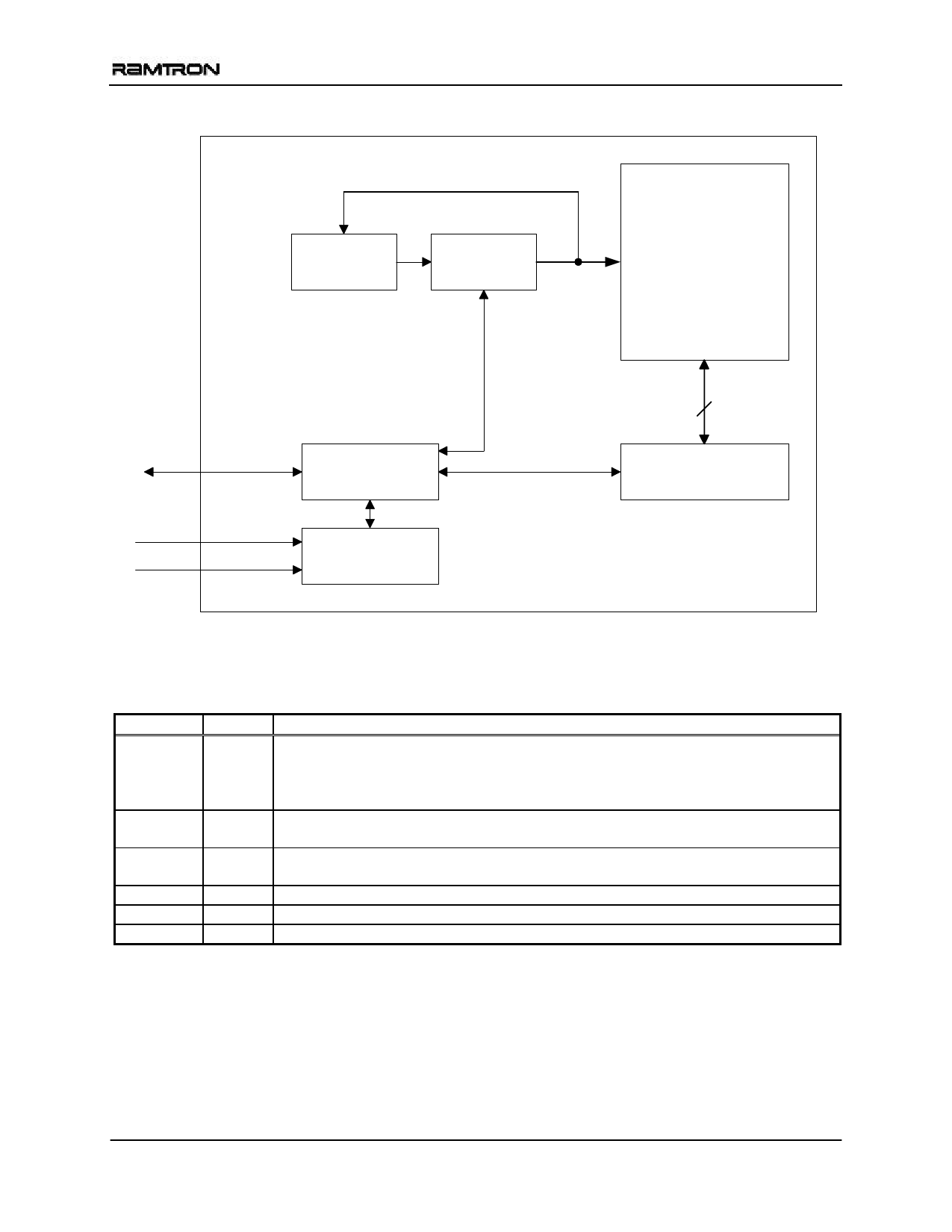
FM24C16A
Counter
Address
Latch
256 x 64
FRAM Array
SDA
`
SCL
WP
Serial to Parallel
Converter
Control Logic
8
Data Latch
Figure 1. Block Diagram
Pin Description
Pin Name
SDA
Type
I/O
SCL
WP
VDD
VSS
NC
Input
Input
Supply
Supply
-
Pin Description
Serial Data Address: This is a bi-directional data pin for the two-wire interface. It
employs an open-drain output and is intended to be wire-OR’d with other devices on the
two-wire bus. The input buffer incorporates a Schmitt trigger for noise immunity and the
output driver includes slope control for falling edges. A pull-up resistor is required.
Serial Clock: The serial clock input for the two-wire interface. Data is clocked-out on
the falling edge and clocked-in on the rising edge.
Write Protect: When WP is high, the entire array is write-protected. When WP is low,
all addresses may be written. This pin is internally pulled down.
Supply Voltage (5V)
Ground
No connect
Rev 3.0
Mar. 2005
Page 2 of 12
Share Link: 