MT4LC4M16R6TG-6S Просмотр технического описания (PDF) - Micron Technology
Номер в каталоге
Компоненты Описание
производитель
MT4LC4M16R6TG-6S Datasheet PDF : 24 Pages
| |||
GENERAL DESCRIPTION
The 4 Meg x 16 DRAM is a high-speed CMOS,
dynamic random-access memory device containing
67,108,864 bits and designed to operate from 3V to
3.6V. The device is functionally organized as 4,194,304
locations containing 16 bits each. The 4,194,304
memory locations are arranged in 4,096 rows by 1,024
columns on the MT4LC4M16R6 or 8,192 rows by 512
columns on the MT4LC4M16N3. During READ or WRITE
cycles, each location is uniquely addressed via the
address bits: 12 row-address bits (A0-A11) and 10
column-address bits (A0-A9) on the MT4LC4M16R6 or
13 row-address bits (A0-A12) and 9 column-address bits
(A0-A8) on the MT4LC4M16N3 version. In addition,
both byte and word accesses are supported via the two
CAS# pins (CASL# and CASH#).
The CAS# functionality and timing related to ad-
dress and control functions (e.g., latching column
addresses or selecting CBR REFRESH) is such that the
internal CAS# signal is determined by the first external
CAS# signal (CASL# or CASH#) to transition LOW and
4 MEG x 16
EDO DRAM
the last to transition back HIGH. The CAS# functional-
ity and timing related to driving or latching data is such
that each CAS# signal independently controls the asso-
ciated eight DQ pins.
The row address is latched by the RAS# signal, then
the column address is latched by CAS#. This device
provides EDO-PAGE-MODE operation, allowing for fast
successive data operations (READ, WRITE or READ-
MODIFY-WRITE) within a given row.
The 4 Meg x 16 DRAM must be refreshed periodi-
cally in order to retain stored data.
DRAM ACCESS
Each location in the DRAM is uniquely addressable,
as mentioned in the General Description. Use of both
CAS# signals results in a word access via the 16 I/O pins
(DQ0-DQ15). Using only one of the two signals results
in a BYTE access cycle. CASL# transitioning LOW se-
lects an access cycle for the lower byte (DQ0-DQ7), and
CASH# transitioning LOW selects an access cycle for
4 Meg x 16 EDO DRAM
D29_2.p65 – Rev. 5/00
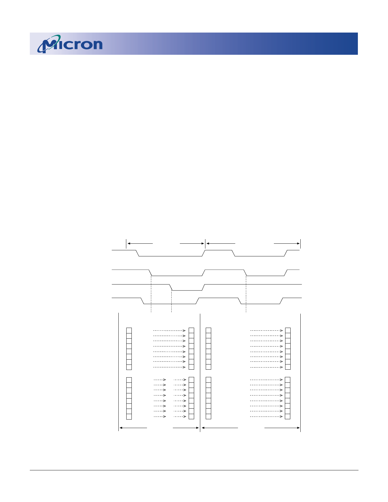
RAS#
WORD WRITE
LOWER BYTE WRITE
CASL#
CASH#
WE#
LOWER BYTE
(DQ0-DQ7)
OF WORD
STORED
DATA
1
1
0
1
1
1
1
1
INPUT
DATA
0
0
1
0
0
0
0
0
INPUT
DATA
STORED
DATA
0
0
1
0
0
0
0
0
STORED
DATA
0
0
1
0
0
0
0
0
INPUT
DATA
1
1
0
1
1
1
1
1
INPUT
DATA
STORED
DATA
1
1
0
1
1
1
1
1
0
X
1
1
1
X
1
1
X
0
0
0
X
0
UPPER BYTE
0
X
1
1
1
X
1
(DQ8-DQ15)
1
X
0
0
0
X
0
OF WORD
0
X
1
1
1
X
1
0
X
1
1
1
X
1
0
X
1
1
1
X
1
0
X
1
1
1
X
1
ADDRESS 0
X = NOT EFFECTIVE (DON'T CARE)
ADDRESS 1
Figure 1
WORD and BYTE WRITE Example
3
Micron Technology, Inc., reserves the right to change products or specifications without notice.
©2000, Micron Technology, Inc.
Share Link: 