FAN6751MR Просмотр технического описания (PDF) - Fairchild Semiconductor
Номер в каталоге
Компоненты Описание
производитель
FAN6751MR Datasheet PDF : 13 Pages
| |||
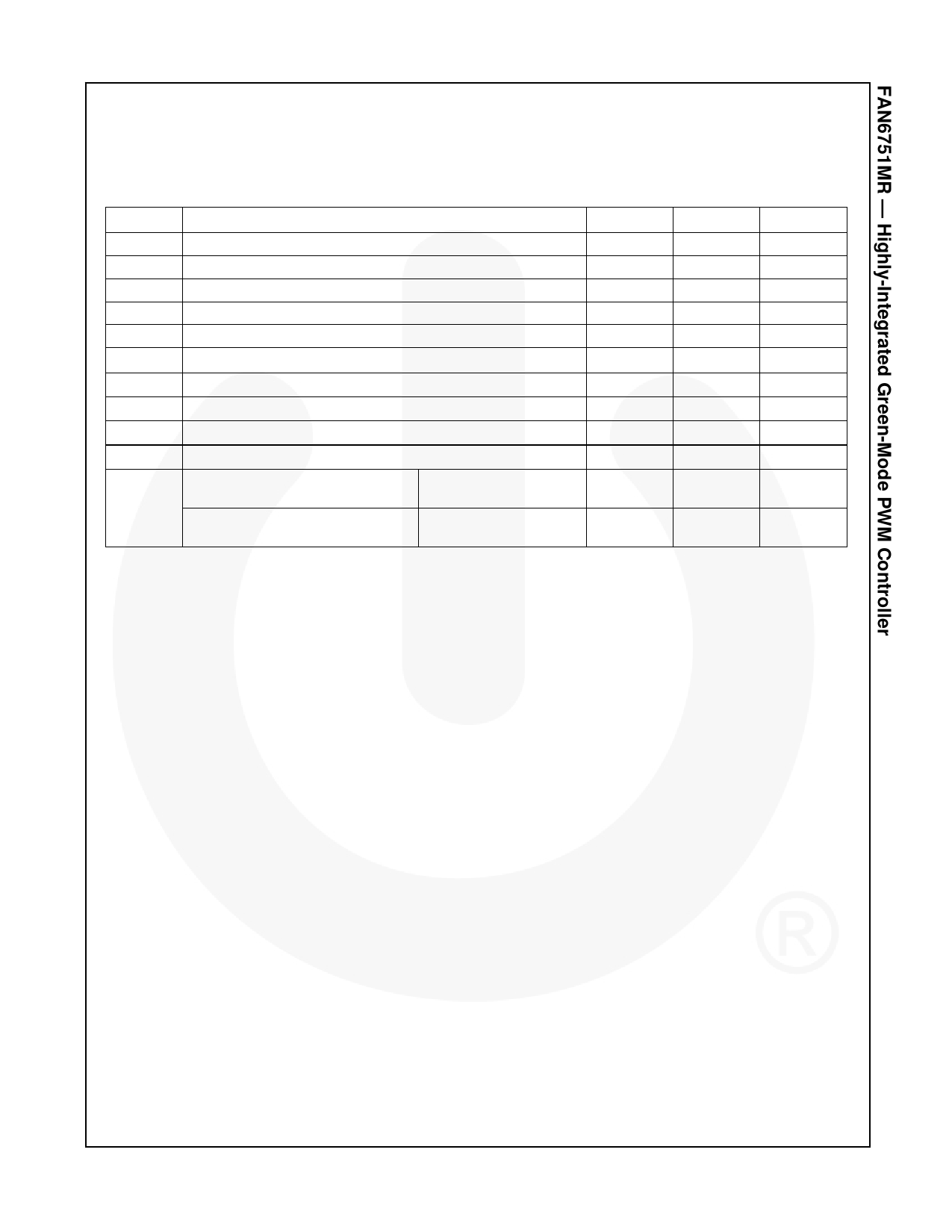
Absolute Maximum Ratings
Stresses exceeding the absolute maximum ratings may damage the device. The device may not function or be
operable above the recommended operating conditions and stressing the parts to these levels is not recommended.
In addition, extended exposure to stresses above the recommended operating conditions may affect device
reliability. The absolute maximum ratings are stress ratings only.
Symbol
Parameter
VDD
DC Supply Voltage(1, 2)
Min.
Max.
30
Unit
V
VFB
VSENSE
FB Pin Input Voltage
SENSE Pin Input Voltage
-0.3
7.0
V
-0.3
7.0
V
VVIN VIN Pin Input Voltage
-0.3
7.0
V
VHV HV Pin Input Voltage
PD
Power Dissipation (TA<50°C)
500
V
400
mW
ΘJA Thermal Resistance, Junction-to-Air
141
°C/W
TJ
Operating Junction Temperature
-40
+150
°C
TSTG Storage Temperature Range
-55
+150
°C
TL
Lead Temperature (Wave Soldering or IR, 10 Seconds)
+260
°C
ESD
Electrostatic Discharge Capability,
Human Body Model: JESD22-A114
Electrostatic Discharge Capability,
Machine Model: JESD22-A115
All pins except HV pin
All pins except HV pin
4
kV
200
V
Notes:
1. All voltage values, except differential voltages, are given with respect to the network ground terminal.
2. Stresses beyond those listed under Absolute Maximum Ratings may cause permanent damage to the device.
© 2008 Fairchild Semiconductor Corporation
FAN6751MR • Rev. 1.0.0
4
www.fairchildsemi.com
Share Link: 