ESDALC6V1-1M2 Просмотр технического описания (PDF) - STMicroelectronics
Номер в каталоге
Компоненты Описание
производитель
ESDALC6V1-1M2
STMicroelectronics

ESDALC6V1-1M2 Datasheet PDF : 11 Pages
| |||
Recommendation on PCB assembly
4
Recommendation on PCB assembly
ESDALC6V1-1M2
4.1
Stencil opening design
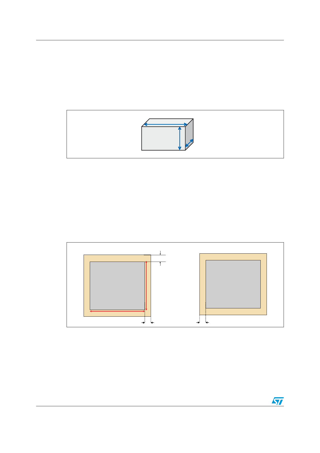
1. General recommendation on stencil opening design
a) Stencil opening dimensions: L (Length), W (Width), T (Thickness).
Figure 17. Stencil opening dimensions
L
TW
b) General design rule
Stencil thickness (T) = 75 ~ 125 µm
Aspect
Ratio
=
W-----
T
≥ 1.5
Aspect Area = 2----T---L-(---L-×---+-W----W-------) ≥ 0.66
2. Reference design
a) Stencil opening thickness: 100 µm
b) Stencil opening for leads: Opening to footprint ratio - between 60% and 65%.
Figure 18. Recommended stencil windows position
Package footprint
Lead footprint on PCB
0.055 mm
Lead footprint on PCB
Stencil window
position
0.39 mm
Stencil window
position
0.45 mm
0.05 mm
0.05 mm
4.2
Solder paste
1. Halide-free flux qualification ROL0 according to ANSI/J-STD-004.
2. “No clean” solder paste is recommended.
3. Offers a high tack force to resist component movement during high speed.
4. Solder paste with fine particles: powder particle size is 20-45 µm.
8/11
Doc ID 12385 Rev 7
Share Link: