EM78869 Просмотр технического описания (PDF) - ELAN Microelectronics
Номер в каталоге
Компоненты Описание
производитель
EM78869 Datasheet PDF : 38 Pages
| |||
EM78869
8-Bit RISC Type Microprocessor
6 Functional Descriptions
6.1 Operational Registers
6.1.1 R0 (Indirect Address Register)
R0 is not a physically implemented register. It is useful as indirect addressing pointer. Any
instruction using R0 as register actually accesses data pointed by the RAM Select Register (R4).
6.1.2 R1 (TCC)
Increased by an external signal edge applied to TCC, or by the instruction cycle clock.
Written and read by the program as any other register.
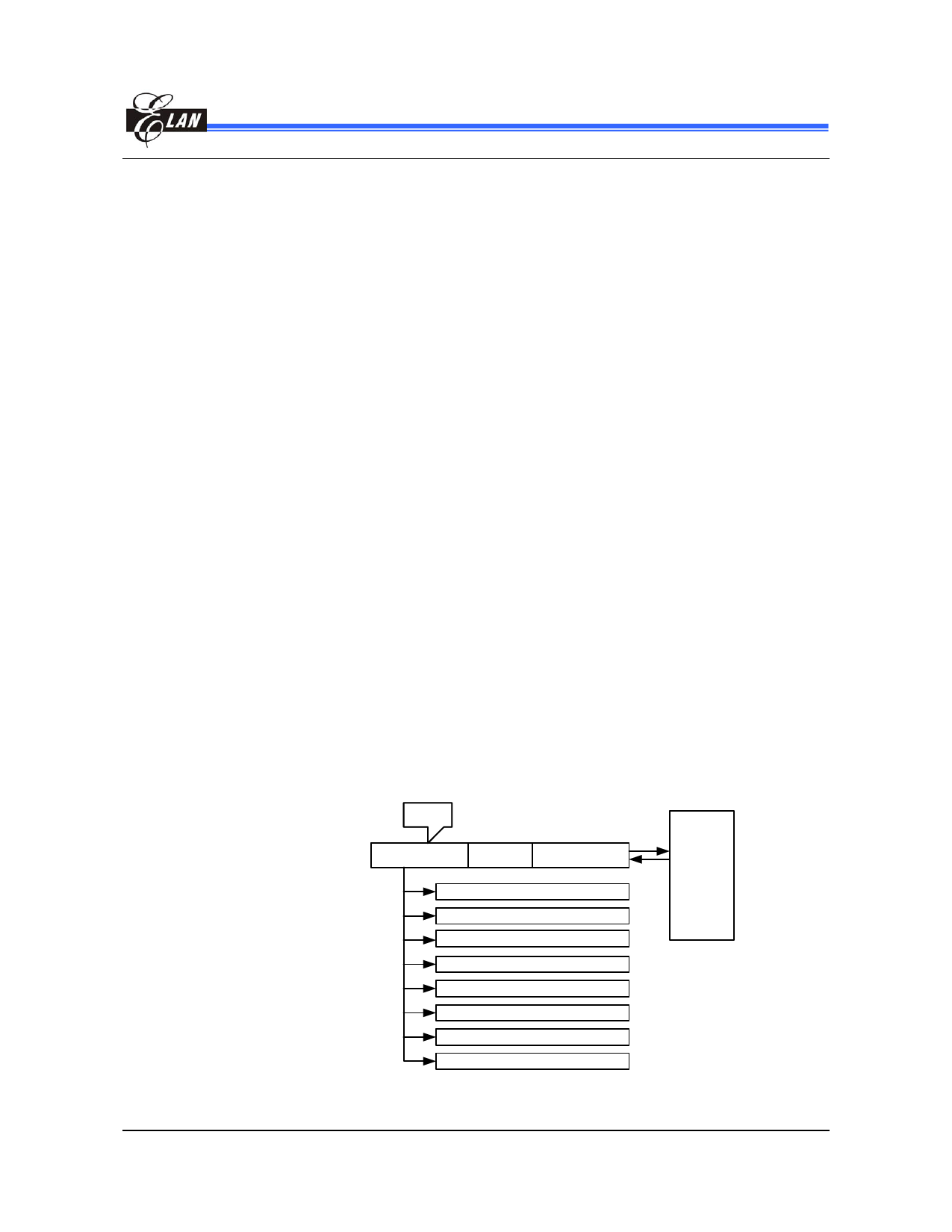
6.1.3 R2 (Program Counter)
The structure is depicted in Fig. 3 below.
Generates 8K × 13 on-chip ROM addresses to the relative programming instruction codes.
"JMP" instruction allows the direct loading of the low 10 program counter bits.
"CALL" instruction loads the low 10 bits of the PC and PC+1, then push it into the stack.
"RET'' ("RETL k," "RETI") instruction loads the program counter with its contents at the top
of stack.
"MOV R2, A" allows the loading of an address from “A” register to the PC, and the 9th and
10th bits are cleared to "0.”
"ADD R2, A" allows a relative address be added into current PC, and its 9th and 10th bits
content are cleared to "0.”
"TBL" allows a relative address to be added into the current PC, and its 9th and 10th bits
content do not change. The most significant bit (A10~A13) will be loaded into the status
register (R5) with the contents of bits PS0~PS3 upon execution of a "JMP,” "CALL,”
"ADD R2, A,” or "MOV R2, A” instruction.
R5
CALL
STACK1
STACK2
PC
A12 A11 A10 A9 A8 A7 ~ A0
STACK3
000 PAGE0 0000~03FF
001 PAGE1 0400~07FF
RET
RETL
RETI
STACK4
STACK5
STACK6
STACK7
STACK8
010 PAGE2 0800~0BFF
011 PAGE3 0C00~0FFF
100 PAGE4 1000~13FF
101 PAGE5 1400~17FF
110 PAGE6 1800~1BFF
111 PAGE7 1C00~1FFF
Fig. 3 Program Counter Organization
This specification is subject to change without further notice.
07.12.2004 (V1.0) 5 of 34
Share Link: 