EL5211A Просмотр технического описания (PDF) - Intersil
Номер в каталоге
Компоненты Описание
производитель
EL5211A Datasheet PDF : 11 Pages
| |||
EL5211A
Electrical Specifications VS+ = +15V, VS- = 0V, RL = 1kΩ to 7.5V, TA = 25°C, unless otherwise specified (Continued)
PARAMETER
DESCRIPTION
CONDITION
MIN TYP MAX
CMRR
Common-Mode Rejection Ratio
AVOL
Open-Loop Gain
OUTPUT CHARACTERISTICS
for VIN from -0.5V to 15.5V
0.5V ≤ VOUT ≤ 14.5V
53
72
60
70
VOL
Output Swing Low
VOH
Output Swing High
ISC
Short-Circuit Current
IOUT
Output Current
POWER SUPPLY PERFORMANCE
IL = -5mA
IL = 5mA
100
200
14.8 14.9
±125
±65
PSRR
Power Supply Rejection Ratio
IS
Supply Current
DYNAMIC PERFORMANCE
VS is moved from 4.5V to 15.5V
No load
60
80
5
7.5
SR
Slew Rate (Note 8)
1V ≤ VOUT ≤ 14V, 20% to 80%
75
tS
Settling to +0.1% (AV = +1)
(AV = +1), VO = 2V step
80
BW
-3dB Bandwidth
60
GBWP
Gain-Bandwidth Product
32
PM
Phase Margin
50
CS
Channel Separation
f = 5MHz
110
dG
Differential Gain (Note 9)
RF = RG = 1kΩ and VOUT = 1.4V
0.16
dP
Differential Phase (Note 9)
RF = RG = 1kΩ and VOUT = 1.4V
0.22
NOTES:
7. Measured over operating temperature range
8. Slew rate is measured on rising and falling edges
9. NTSC signal generator used
UNIT
dB
dB
mV
V
mA
mA
dB
mA
V/µs
ns
MHz
MHz
°
dB
%
°
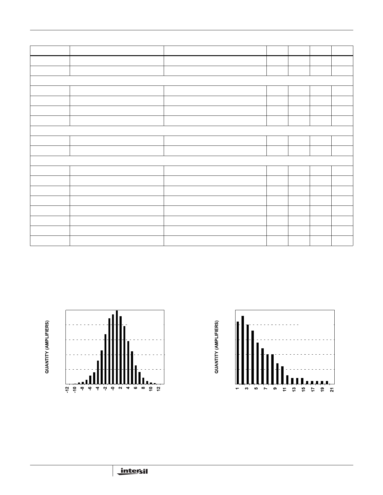
Typical Performance Curves
500
VS=±5V
TA=25°C
400
TYPICAL
PRODUCTION
DISTRIBUTION
300
200
100
0
INPUT OFFSET VOLTAGE (mV)
FIGURE 1. INPUT OFFSET VOLTAGE DISTRIBUTION
25
VS=±5V
20
TYPICAL
PRODUCTION
DISTRIBUTION
15
10
5
0
INPUT OFFSET VOLTAGE DRIFT, TCVOS (µV/°C)
FIGURE 2. INPUT OFFSET VOLTAGE DRIFT
4
FN6143.0
June 15, 2005
Share Link: 