EL4451 Просмотр технического описания (PDF) - Intersil
Номер в каталоге
Компоненты Описание
производитель
EL4451 Datasheet PDF : 10 Pages
| |||
EL4451
package chosen. This is a close estimate for the dissipation
of a circuit:
PD = 2 × VS × IS, max + (VS - VO) × VO/RPAR
where
IS, max is the maximum supply current
VS is the ± supply voltage (assumed equal)
VO is the output voltage
RPAR is the parallel of all resistors loading the output
For instance, the EL4451 draws a maximum of 18mA. With
light loading, RPAR →∞ and the dissipation with ±5V
supplies is 180mW. The maximum supply voltage that the
device can run on for a given PD and other parameters is:
VS, max = (PD + VO2/RPAR) / (2IS + VO/RPAR)
The maximum dissipation a package can offer is:
PD, max = (TJ, max-TA, max) / θJA
Where
TJ,max is the maximum die temperature, 150°C for
reliability, less to retain optimum electrical performance
TA,max is the ambient temperature, 70°C for commercial
and 85°C for industrial range
θJAis the thermal resistance of the mounted package,
obtained from data sheet dissipation curves
The more difficult case is the SO-14 package. With a
maximum die temperature of 150°C and a maximum
ambient temperature of 85°C, the 65°C temperature rise and
package thermal resistance of 120°C/W gives a dissipation
of 542mW at 85°C. This allows the full maximum operating
supply voltage unloaded, but reduced if loaded.
Output Loading
The output stage of the EL4451 is very powerful. It typically
can source 80mA and sink 120mA. Of course, this is too
much current to sustain and the part will eventually be
destroyed by excessive dissipation or by metal traces on the
die opening. The metal traces are completely reliable while
delivering the 30mA continuous output given in the Absolute
Maximum Ratings table in this data sheet, or higher purely
transient currents.
Gain changes only 0.2% from no load to 100Ω load. Heavy
resistive loading will degrade frequency response and video
distortion for loads < 100Ω.
Capacitive loads will cause peaking in the frequency
response. If capacitive loads must be driven, a small-valued
series resistor can be used to isolate it. 12Ω to 51Ω should
suffice. A 22Ω series resistor will limit peaking to 2.5dB with
even a 220pF load.
Leveling Circuits
Often a variable-gain control is used to normalize an input
signal to a standard amplitude from a modest range of
possible input amplitude. A good example is in video
systems, where an unterminated cable will yield a twice-
sized standard video amplitude, and an erroneously twice-
terminated cable gives a 2/3-sized input.
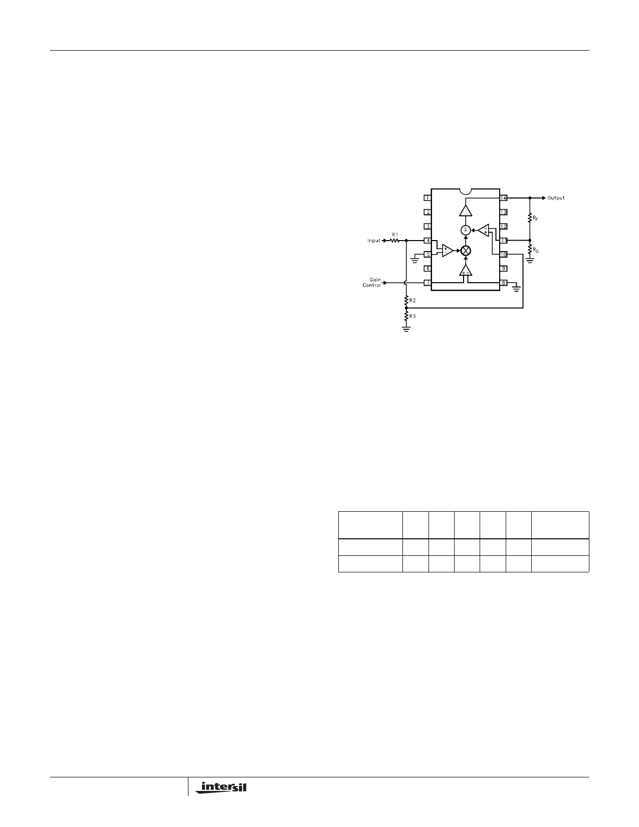
Here is a ±6dB range preamplifier:
FIGURE 1. LINEARIZED LEVELING AMPLIFIER
In this arrangement, the EL4451 outputs a mixture of the
signal routed through the multiplier and the REF terminal.
The multiplier port produces the most distortion and needs
to handle a fraction of an oversized video input, whereas the
REF port is just like an op-amp input summing into the
output. Thus, for oversized inputs the gain will be decreased
and the majority of the signal is routed through the linear
REF terminal. For undersized inputs, the gain is increased
and the multiplier’s contribution added to the output.
Here are some component values for two designs:
ATTENUATION
-3dB
RATIO
RF RG R1 R2 R3 BANDWIDTH
1.5
200Ω 400Ω 300Ω 100Ω 200Ω 47MHz
2
400Ω 400Ω 500Ω 100Ω 200Ω 28MHz
8
Share Link: 