MB86435 Просмотр технического описания (PDF) - Fujitsu
Номер в каталоге
Компоненты Описание
производитель
MB86435 Datasheet PDF : 36 Pages
| |||
MB86435
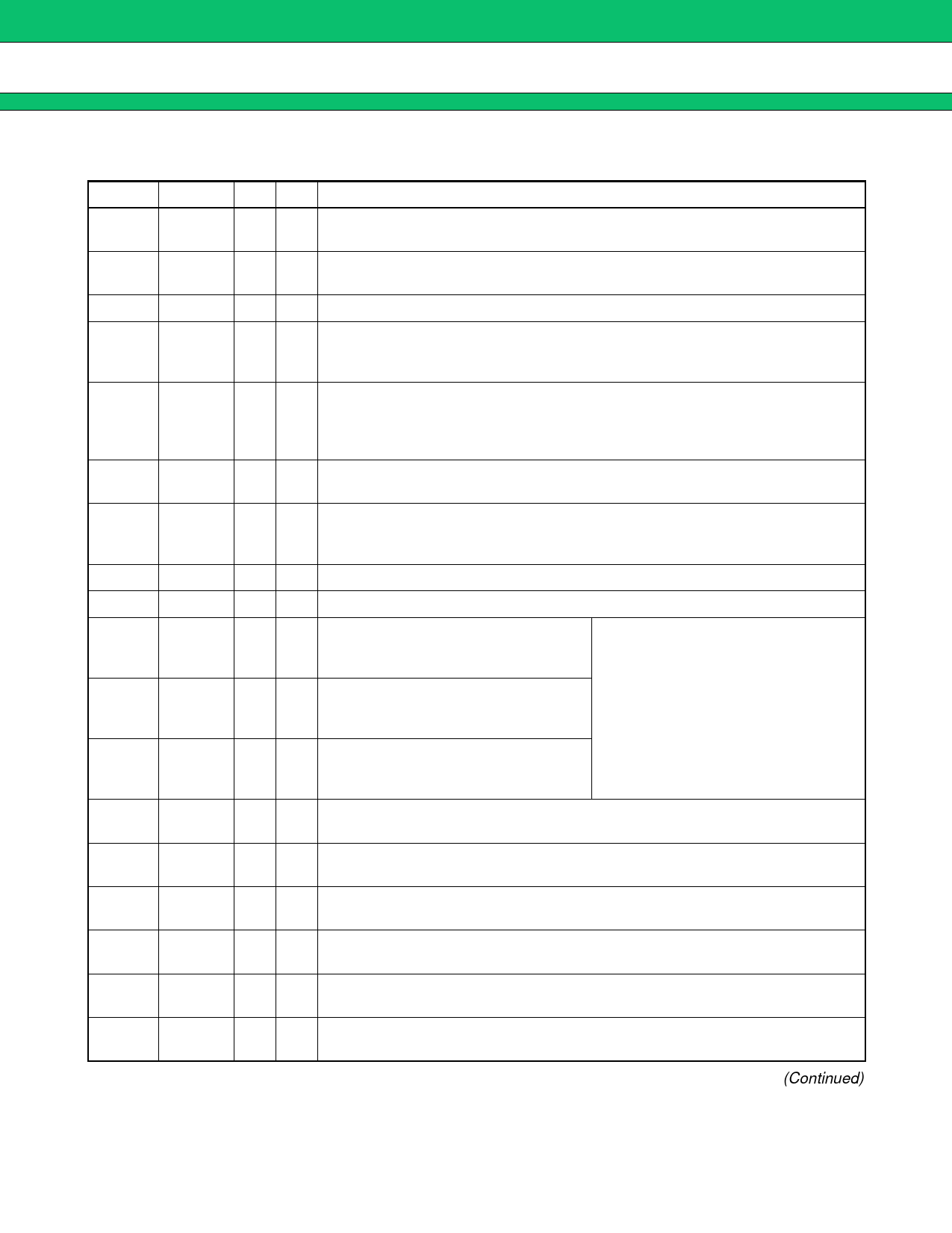
s PIN DESCRIPTION
Pin No. Symbol I/O A/D
Description
1
VRH
O
A
Bypass capacitor connector pin for the A/D D/A reference voltage generator
circuit. Place capacitor between VRH and CAG pins.
2
SGC
O
A
Bypass capacitor connector pin for the signal ground potential generator
circuit. Place capacitor between SGC and CAG pins.
3
VDDAC P A Analog power supply pin for codec block. To be set within range 2.7 to 3.6 V.
PCM codec send/receive synchronization signal input pin. Operating clock
6
SYNC I D frequency 8 kHz. CMOS interface. Constant H/L level signal will cause part of
codec block to power-down.
Send/receive PCM signal series bit rate setting input pin. Data rate for µ-law,
7
CLK
I
D
A-law modes may be set to any level in the range 64 k to 3.152 MHz, and for
linear mode in the range 256 k to 3.152 MHz. Constant H or L level signal will
cause part of codec block to power-down. CMOS interface.
8
DIN
I
D
PCM signal input pin. This signal is picked up internally at the fall of the CLK
signal. CMOS interface.
PCM signal output pin. Data is output in sync with the rise of the CLK signal.
9
DOUT O D After data output, loses PLL synchronization, and at power-down this signal is
fixed at H level. CMOS interface.
10
VDD P D Digital power supply pin. To be set within range 2.7 to 3.6 V.
11
DG
G D Digital ground pin. To be set to 0V.
Power-down control signal input pin.
12
PSC0 I D CMOS interface. Used with PSC1,2
pins for power-down settings.
PSC 2 1 0
Power-down control signal input pin.
13
PSC1 I D CMOS interface. Used with PSC0,2
pins for power-down settings.
000
100
—1 0
—— 1
Full power-down
VREF operating
Tone operating
All operations available
Power-down control signal input pin. (—: value not determined)
14
PSC2 I D CMOS interface. Used with PSC0,1
pins for power-down settings.
15
SRD
I
D
9-bit serial data input pin. CMOS interface. Data is written at the rise of the
signal from this pin.
16
SRC
I
D
Clock input pin for 9-bit serial data writing. CMOS interface. Data is written at
the rise of this pin.
17
STB
I
D
Serial data latch strobe signal. Data is latched by the L level signal. CMOS
interface.
18
XPRST I
D
Digital reset signal input pin. CMOS interface. L level: internal latch initialization
H level: normal operation
19
LO0
O
D
External control latch output pin. Outputs value D0 of address 1000. CMOS
interface.
20
LO1
O
D
External control latch output pin. Outputs value D1 of address 1000. CMOS
interface.
(Continued)
3
Share Link: 