EDI8L3265C Просмотр технического описания (PDF) - White Electronic Designs Corporation
Номер в каталоге
Компоненты Описание
производитель
EDI8L3265C Datasheet PDF : 6 Pages
| |||
Absolute Maximum Ratings*
Voltage on any pin relative to VSS
Operating Temperature TA (Ambient)
Commercial
Industrial
Storage Temperature
Power Dissipation
Output Current.
Junction Temperature, TJ
-0.5V to 7.0V
0°C to + 70°C
-40°C to +85°C
-55°C to +125°C
3.0 Watts
20 mA
175°C
*Stress greater than those listed under "Absolute Maximum Ratings" may cause permanent
damage to the device. This is a stress rating only and functional operation of the device at
these or any other conditions greater than those indicated in the operational sections of this
specification is not implied. Exposure to absolute maximum rating conditions for extended
periods may affect reliability.
EDI8L3265C
64Kx32 SRAM
Recommended DC Operating Conditions
Parameter
Sym Min Typ Max
Units
Supply Voltage VCC 4.75 5.0 5.25
V
Supply Voltage VSS 0 0 0
V
Input High Voltage VIH 2.2 -- VCC+0.5 V
Input Low Voltage VIL -0.3 -- 0.8
V
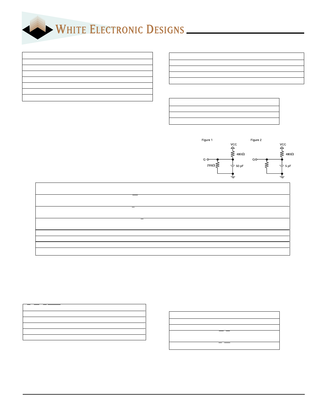
AC Test Conditions
Input Pulse Levels
Input Rise and Fall Times
Input and Output Timing Levels
Output Load
VSS to 3.0V
5ns
1.5V
Figure 1
(note: For TEHQZ,TGHQZ and TWLQZ, CL = 5pF)
DC Electrical Characteristics
Parameter
Sym
Conditions
Min
Operating Power
Supply Current
Standby (TTL)
Supply Current
Full Standby
Supply Current CMOS
Input Leakage Current
Output Leakage Current
Output High Volltage
Output Low Voltage
ICC1
ICC2
ICC3
ILI
ILO
VOH
VOL
W= VIL, II/O = 0mA,
Min Cycle
E ³ VIH, VIN £ VIL or
VIN ³ VIH, f=ØMHz
E ³ VCC-0.2V
VIN ³ VCC-0.2V or VIN £ 0.2V
VIN = 0V to VCC
V I/O = 0V to VCC
IOH = -4.0mA
2.4
IOL = 8.0mA
*Typical: TA = 25°C, VCC = 5.0V
*Advanced Information
Max
12ns* 15ns 20/25ns
500 460 420
60 60 60
20 20 20
±10 ±10 ±10
±10 ±10 ±10
0.4 0.4 0.4
Unit
ns
mA
mA
mA
µA
µA
V
V
Truth Table
E W G BSØ-3
HX X X
LHH X
LXX H
LHL L
LLX L
X Means Don't Care
Mode
Standby
Output Disable
Output Disable
Read
Write
Output
High Z
High Z
High Z
Dout
Din
Power
ICC2,ICC3
ICC1
ICC1
ICC1
ICC1
Capacitance
(f=1.0MHz, VIN=VCC or VSS)
Parameter
Address Lines
Data Lines
Write & Output
Enable Lines
Chip Enable Lines
Sym
CA
CD/Q
W, G
E, BS
Max
20
10
16
9
These parameters are sampled, not 100% tested.
Unit
pF
pF
pF
bF
pF
White Electronic Designs Corporation (602) 437-1520 www.whiteedc.com
2
Share Link: 