RF2140 Просмотр технического описания (PDF) - RF Micro Devices
Номер в каталоге
Компоненты Описание
производитель
RF2140 Datasheet PDF : 12 Pages
| |||
RF2140
Theory of Operation and Application Information
The RF2140 is a three-stage device with 28 dB gain at
full power. Therefore, the drive required to fully satu-
rate the output is +5dBm. Based upon HBT (Hetero-
junction Bipolar Transistor) technology, the part
2
requires only a single positive 3V supply to operate to
full specification. Power control is provided through a
single pin interface, with a separate Power Down con-
trol pin. The final stage ground is achieved through the
large pad in the middle of the backside of the package.
First and second stage grounds are brought out
through separate ground pins for isolation from the out-
put. These grounds should be connected directly with
vias to the PCB ground plane, and not connected with
the output ground to form a so called “local ground
plane” on the top layer of the PCB. The output is
brought out through the wide output pad, and forms the
RF output signal path.
The amplifier operates in near Class C bias mode. The
final stage is "deep AB", meaning the quiescent current
is very low. As the RF drive is increased, the final stage
self-biases, causing the bias point to shift up and, at
full power, draws about 1500mA. The optimum load for
the output stage is approximately 4.5Ω. This is the load
at the output collector, and is created by the series
inductance formed by the output bond wires, vias, and
microstrip, and 2 shunt capacitors external to the part.
The optimum load impedance at the RF Output pad is
4.5-j3.9Ω. With this match, a 50Ω terminal impedance
is achieved. The input is internally matched to 50Ω
with just a blocking capacitor needed. This data sheet
defines the configuration for GSM operation.
The input is DC coupled; thus, a blocking cap must be
inserted in series. Also, the first stage bias may be
adjusted by a resistive divider with high value resistors
on this pin to VPC and ground. For nominal operation,
however, no external adjustment is necessary as inter-
nal resistors set the bias point optimally.
When the device is driven at maximum input power self
biasing would occur. This results in less isolation than
one would expect, and the maximum output power
would be about -15dBm. If the drive power to the PA is
turned on before the GSM ramp-up, higher isolation is
required. In order to meet the GSM system specs
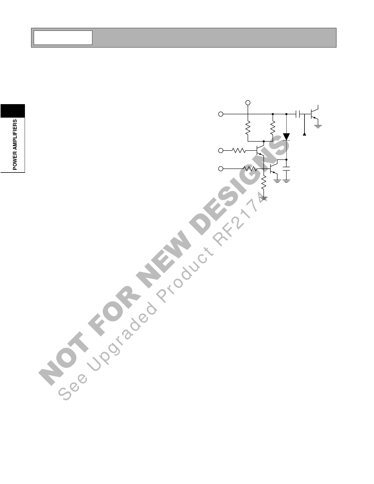
under those conditions, a PIN diode attenuator con-
nected to the input can be turned on. The figure below
shows how the attenuator and its controls are con-
nected.
VCC
RF IN
APC
AT_EN
750 Ω 500 Ω
5 kΩ
2 kΩ
PIN
From Bias
Stages
The current through the PIN diode is controlled by two
signals: AT_EN and APC. The AT_EN signal allows
current through the PIN diode and is an on/off function.
The APC signal controls the amount of current through
the PIN diode. Normally, the AT_EN signal will be
derived from the VCO ENABLE signal available in
most GSM handset designs. If maximum isolation is
needed before the ramp-up, the AT_EN signal needs to
be turned on before the RF power is applied to the
device input. The current into this pin is not critical, and
can be reduced to a few hundred micro amps with an
external series resistor. Without the resistor, the pin will
draw about 700µA.
Because of the inverting stage at the APC input, the
current through the PIN diode is inverted from the APC
voltage. Thus, when VAPC is high for maximum output
power, the attenuator is turned off to obtain maximum
drive level for the first RF stage. When VAPC is low for
maximum isolation, the attenuator is be turned on to
reduce the drive level and to avoid self-biasing.
The PIN diode is dimensioned such that a low VAPC the
impedance of the diode is about 50 Ohm. Since the
input impedance of the first RF stage become very
high when the bias is turned off, this topology will main-
tain a good input impedance over the entire VAPC con-
trol range.
VCC1 and VCC2 provide supply voltage to the first and
second stage, as well as provides some frequency
selectivity to tune to the operating band. Essentially,
2-134
Rev A12 011031
Share Link: 