LT1529CT-3.3 Просмотр технического описания (PDF) - Linear Technology
Номер в каталоге
Компоненты Описание
производитель
LT1529CT-3.3
Linear Technology

LT1529CT-3.3 Datasheet PDF : 12 Pages
| |||
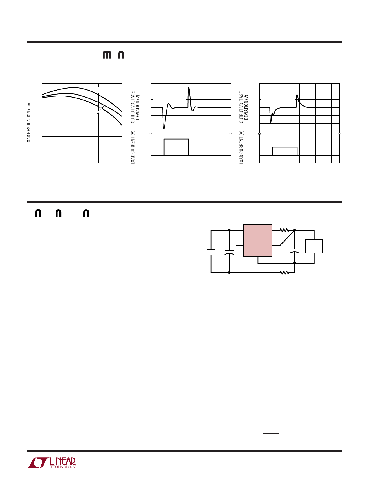
TYPICAL PERFOR A CE CHARACTERISTICS
LT1529
LT 1529-3.3/LT 1529-5
Load Regulation
5
0
LT1529-5
–5
LT1529-3.3
LT1529
–10
–15
–20 VIN = VOUT (NOMINAL) + 1V
∆ILOAD = 100mA to 3A
VADJ = VOUT
– 25
– 50 – 25 0 25 50 75
TEMPERATURE (°C)
100 125
LT1529 • G28
LT1529-5 Transient Response
0.2
VIN = 6V
CIN = 3.3µF TANT
0.1 COUT = 47µF TANT
0
– 0.1
– 0.2
3
2
1
0 100 200 300 400 500 600 700 800 900 1000
TIME (µs)
LT1529 • G29
LT1529-5 Transient Response
VIN = 6V
0.2 CIN = 10µF TANT
0.1 COUT = 4.7µF TANT
0
– 0.1
– 0.2
3
2
1
0 20 40 60 80 100 120 140 160 180 200
TIME (µs)
LT1529 • G30
PI FU CTIO S
OUTPUT (Pin 1): OUTPUT Pin. The OUTPUT pin supplies
power to the load. A minimum output capacitor of 3.3µF is
required to prevent oscillations. Larger values will be
required to optimize transient response for large load
current deltas. See the Applications Information section
for further information on output capacitance and reverse
output characteristics.
SENSE (Pin 2): SENSE Pin. For fixed voltage versions of
the LT1529 (LT1529-3.3, LT1529-5) the SENSE pin is the
input to the error amplifier. Optimum regulation will be
obtained at the point where the SENSE pin is connected to
the output pin. For most applications the SENSE pin is
connected directly to the OUTPUT pin at the regulator. In
critical applications small voltage drops caused by the
resistance (RP) of PC traces between the regulator and the
load, which would normally degrade regulation, may be
eliminated by connecting the SENSE pin to the OUTPUT
pin at the load as shown in Figure 1 (Kelvin Sense Connec-
tion). Note that the voltage drop across the external PC
traces will add to the dropout voltage of the regulator. The
SENSE pin bias current is 15µA at the nominal regulated
output voltage. This pin is internally clamped to – 0.6V
(one VBE).
ADJ (Pin 2): Adjust Pin. For the LT1529 (adjustable
version) the ADJ pin is the input to the error amplifier. This
+
VIN
5
1
VIN OUTPUT
LT1529-5
4
2
SHDN SENSE
GND
3
RP
+
LOAD
RP
LT1529 • F01
Figure 1. Kelvin Sense Connection
pin is internally clamped to 6V and – 0.6V (one VBE). This
pin has a bias current of 150nA which flows into the pin.
See Bias Current curve in the Typical Performance Char-
acteristics. The ADJ pin reference voltage is equal to 3.75V
referenced to ground.
SHDN (Pin 4): Shutdown Pin. This pin is used to put the
device into shutdown. In shutdown the output of the
device is turned off. This pin is active low. The device will
be shut down if the SHDN pin is actively pulled low. The
SHDN pin current with the pin pulled to ground will be 6µA.
The SHDN pin is internally clamped to 7V and – 0.6V (one
VBE). This allows the SHDN pin to be driven directly by 5V
logic or by open-collector logic with a pull-up resistor. The
pull-up resistor is only required to supply the leakage
current of the open-collector gate, normally several mi-
croamperes. Pull-up current must be limited to a maxi-
mum of 5mA. A curve of SHDN pin input current as a
7
Share Link: