LT1529 Просмотр технического описания (PDF) - Linear Technology
Номер в каталоге
Компоненты Описание
производитель
LT1529 Datasheet PDF : 12 Pages
| |||
LT1529
LT 1529-3.3/LT 1529-5
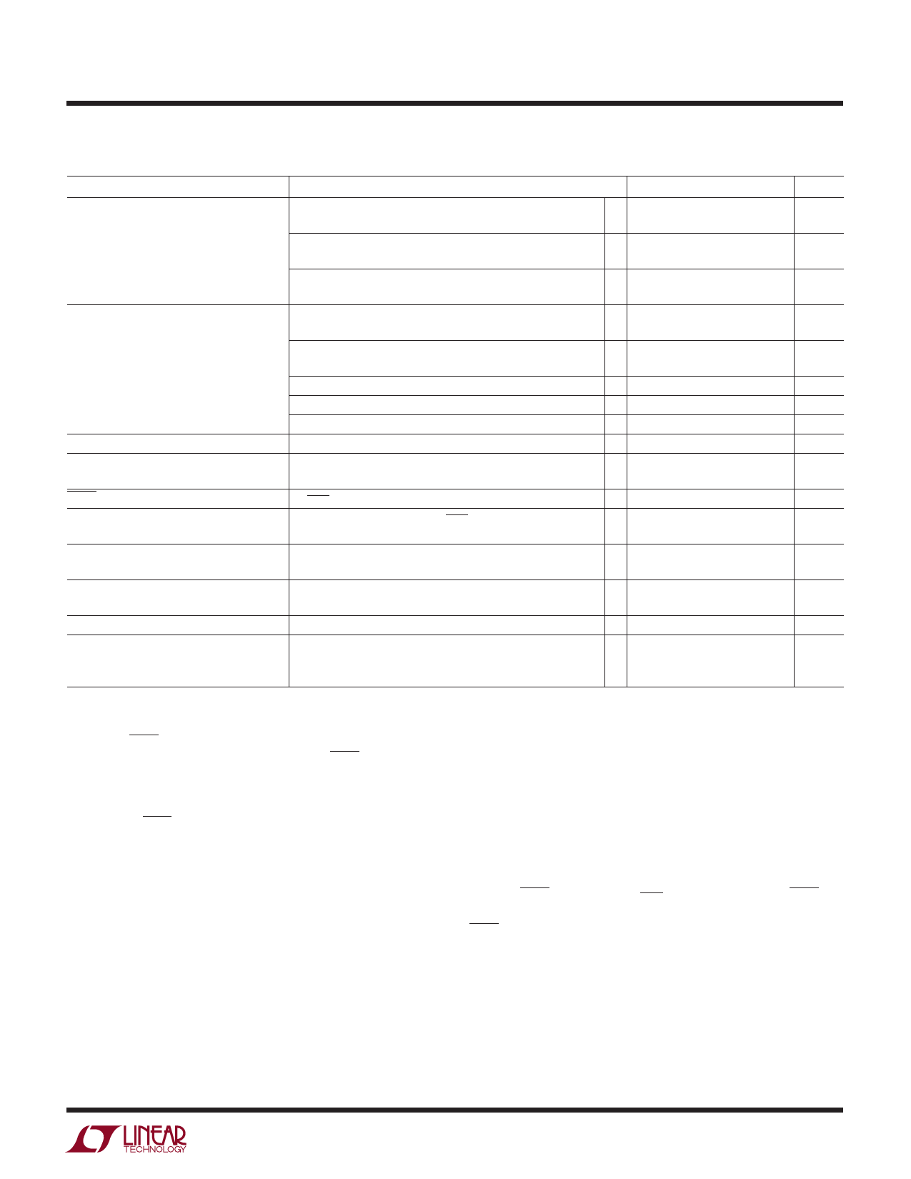
ELECTRICAL CHARACTERISTICS
The q denotes specifications which apply over the operating temperature range, otherwise specificatons are at TA = 25°C. (Note 3)
PARAMETER
Dropout Voltage
(Note 6)
GND Pin Current
(Note 7)
ADJ Pin Bias Current (Notes 5, 9)
Shutdown Threshold
SHDN Pin Current (Note 10)
Quiescent Current in Shutdown
(Note 11)
Ripple Rejection
Current Limit
Input Reverse Leakage Current
Reverse Output Current (Note 12)
CONDITIONS
ILOAD = 700mA, TJ = 25°C
ILOAD = 700mA
ILOAD = 1.5A, TJ = 25°C
ILOAD = 1.5A
ILOAD = 3A, TJ = 25°C
ILOAD = 3A
ILOAD = 0mA, TJ = 25°C
ILOAD = 0mA, TJ = 125°C (Note 8)
ILOAD = 100mA, TJ = 25°C
ILOAD = 100mA, TJ = 125°C (Note 8)
ILOAD = 700mA
ILOAD = 1.5A
ILOAD = 3A
TJ = 25°C
VOUT = Off to On
VOUT = On to Off
VSHDN = 0V
VIN = VOUT (Nominal) + 1V, VSHDN = 0V
VIN – VOUT = 1V (Avg), VRIPPLE = 0.5VP-P,
fRIPPLE = 120Hz, ILOAD = 1.5A
VIN – VOUT = 7V, TJ = 25°C
VIN = VOUT (Nominal) + 1.5V, ∆VOUT = – 0.1V
VIN = – 15V, VOUT = 0V
LT1529-3.3
LT1529-5
LT1529 (Note 6)
VOUT = 3.3V, VIN = 0V
VOUT = 5V, VIN = 0V
VOUT = 3.8V, VIN = 0V
MIN TYP MAX
320
430
q
550
430
550
q
700
600
750
q
950
50
100
400
0.6
1.0
1.0
q
5.5
12
q
20
40
q
80
160
150
300
q
1.20
2.8
q 0.25 0.75
q
4.5
10
q
15
30
50
62
5
q 3.2
4.7
q
1.0
16
16
16
UNITS
mV
mV
mV
mV
mV
mV
µA
µA
mA
mA
mA
mA
mA
nA
V
V
µA
µA
dB
A
A
mA
µA
µA
µA
Note 1: Absolute Maximum Ratings are those values beyond which the life
of a device may be impaired.
Note 2: The SHDN pin input voltage rating is required for a low impedance
source. Internal protection devices connected to the SHDN pin will turn on
and clamp the pin to approximately 7V or – 0.6V. This range allows the use
of 5V logic devices to drive the pin directly. For high impedance sources or
logic running on supply voltages greater than 5.5V, the maximum current
driven into the SHDN pin must be limited to less than 5mA.
Note 3: The device is tested under pulse load conditions such that TJ = TA.
Note 4: Operating conditions are limited by maximum junction
temperature. The regulated output voltage specification will not apply for
all possible combinations of input voltage and output current. When
operating at maximum input voltage, the output current range must be
limited. When operating at maximum output current the input voltage
range must be limited.
Note 5: The LT1529 is tested and specified with the ADJ pin connected to
the OUTPUT pin.
Note 6: Dropout voltage is the minimum input/output voltage required to
maintain regulation at the specified output current. In dropout the output
voltage will be equal to (VIN – VDROPOUT).
Note 7: GND pin current is tested with VIN = VOUT (nominal) and a current
source load. This means that the device is tested while operating in its
dropout region. This is the worst-case GND pin current. The GND pin
current will decrease slightly at higher input voltages.
Note 8: GND pin current will rise at TJ > 75°C. This is due to internal
circuitry designed to compensate for leakage currents in the output
transistor at high temperatures. This allows quiescent current to be
minimized at lower temperatures, yet maintain output regulation at high
temperatures with light loads. See quiescent current curve in typical
performance characteristics.
Note 9: ADJ pin bias current flows into the ADJ pin.
Note 10: SHDN pin current at VSHDN = 0V flows out of the SHDN pin.
Note 11: Quiescent current in shutdown is equal to the sum total of the
SHDN pin current (5µA) and the GND pin current (10µA).
Note 12: Reverse output current is tested with the VIN pin grounded and
the OUTPUT pin forced to the rated output voltage. This current flows into
the OUTPUT pin and out of the GND pin.
3
Share Link: 