DTA143EUA Просмотр технического описания (PDF) - Micro Commercial Components
Номер в каталоге
Компоненты Описание
производитель
DTA143EUA Datasheet PDF : 3 Pages
| |||
MCC
TM
Micro Commercial Components
omponents
20736 Marilla Street Chatsworth
!"#
$%
!"#
DTA143EUA
Features
• Lead Free Finish/RoHS Compliant ("P" Suffix designates
RoHS Compliant. See ordering information)
• Epoxy meets UL 94 V-0 flammability rating
• Moisure Sensitivity Level 1
• Built-in bias resistors enable the configuration of an inverter circuit
without connecting external input resistors
• The bias resistors consist of thin-film resistors with complete
isolation to allow negative biasing of the input. They also have the
advantage of almost completely eliminating parasitic effects.
• Only the on/off conditions need to be set for operation, making
device design easy
• Halogen free available upon request by adding suffix "-HF"
Absolute maximum ratings @ 25к
Symbol
Parameter
Min Typ Max Unit
VCC
VIN
IO
IC(MAX)
Pd
Tj
Supply voltage
Input voltage
Output current
Power dissipation
Junction temperature
--- -50 ---
V
-30 --- 10
V
---
-100
-100
---
mA
--- 200 --- mW
--- 150 ---
ć
Tstg
Storage temperature
-55 --- 150
ć
Electrical Characteristics @ 25к
Symbol
VI(off)
VI(on)
VO(on)
II
IO(off)
GI
R1
R2/R1
fT
Parameter
Input voltage (VCC=-5V, IO=-100A)
(VO=-0.3V, IO=-20mA)
Output voltage (IO/II=-10mA/-0.5mA
Input current (VI=-5V)
Output current (VCC=-50V, VI=0)
DC current gain (VO=-5V, IO=-10mA)
Input resistance
Resistance ratio
Transition frequency
(VCE=-10V, IE=5mA, f=100MHz)
Min Typ
---
---
-3.0 ---
---
---
---
---
---
---
30 ---
3.29 4.7
0.8 1.0
--- 250
Max
-0.5
---
-0.3
-1.8
-0.5
---
6.11
1.2
---
Unit
V
V
V
mA
A
K¡
MHz
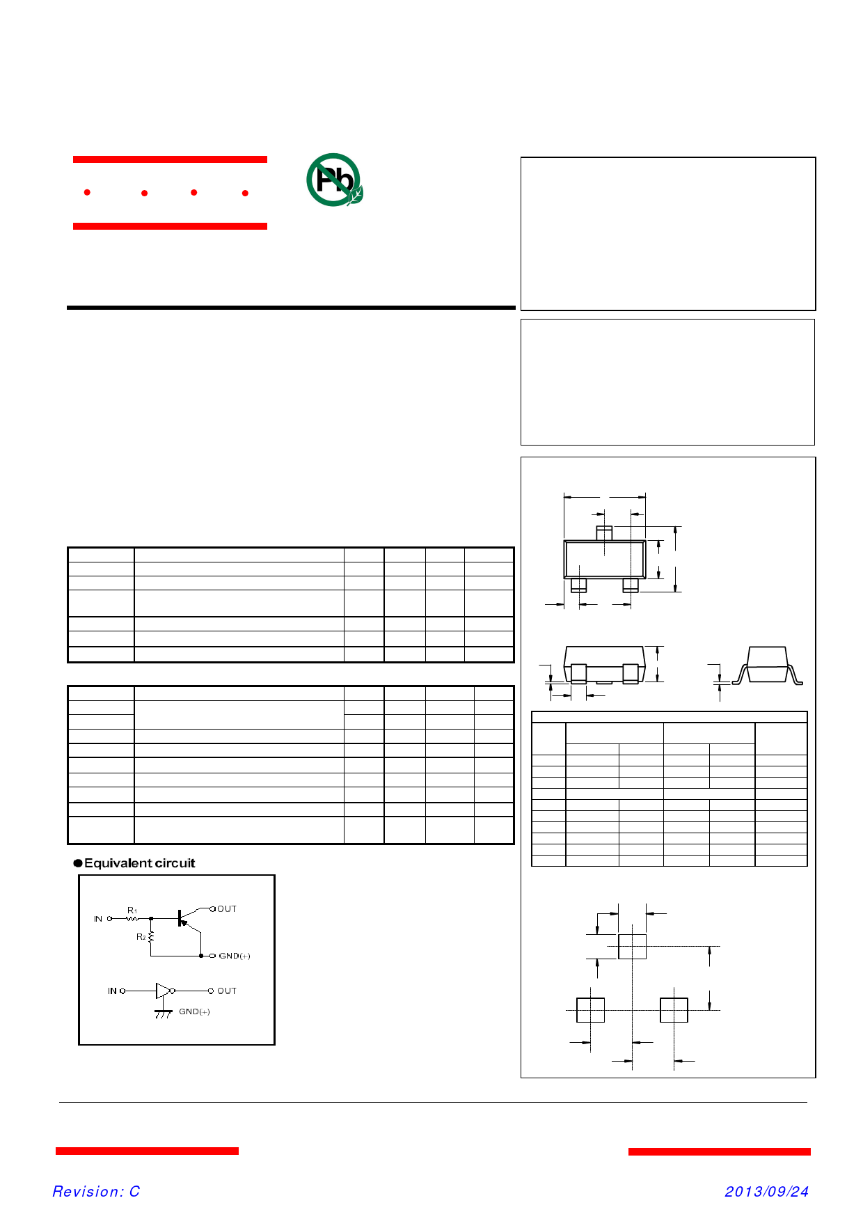
*Marking: 13
PNP
Digital Transistors
SOT-323
A
D
3
BC
12
F
E
1: IN
2: GND
3: OUT
G
H
J
K
DIMENSIONS
INCHES
MM
DIM
MIN
MAX
MIN
MAX
A
.071
.087
1.80
2.20
B
.045
.053
1.15
1.35
C
.083
.096
2.10
2.45
D
.026 Nominal
0.65Nominal
E
.047
.055
1.20
1.40
F
.012
.016
.30
.40
G
.000
.004
.000
.100
H
.035
.039
.90
1.00
J
.004
.010
.100
.250
K
.006
.016
.15
.40
Suggested Solder
Pad Layout
0.70
NOTE
0.90
1.90 mm
0.65
0.65
Revision: C
www.mccsemi.com
1 of 3
2013/09/24
Share Link: 