DS2460 Просмотр технического описания (PDF) - Maxim Integrated
Номер в каталоге
Компоненты Описание
производитель
DS2460 Datasheet PDF : 8 Pages
| |||
Abridged Data Sheet
DS2460
ABSOLUTE MAXIMUM RATINGS
Voltage Range on Any Pin Relative to Ground
Maximum Current Into Any Pin
Operating Temperature Range
Junction Temperature
Storage Temperature Range
Soldering Temperature
-0.5V, +6V
±20mA
-40°C to +85°C
+150°C
-55°C to +125°C
See IPC/JEDEC J-STD-020
Stresses beyond those listed under “Absolute Maximum Ratings” may cause permanent damage to the device. These are stress ratings only,
and functional operation of the device at these or any other conditions beyond those indicated in the operational sections of the specifications is
not implied. Exposure to the absolute maximum rating conditions for extended periods may affect device.
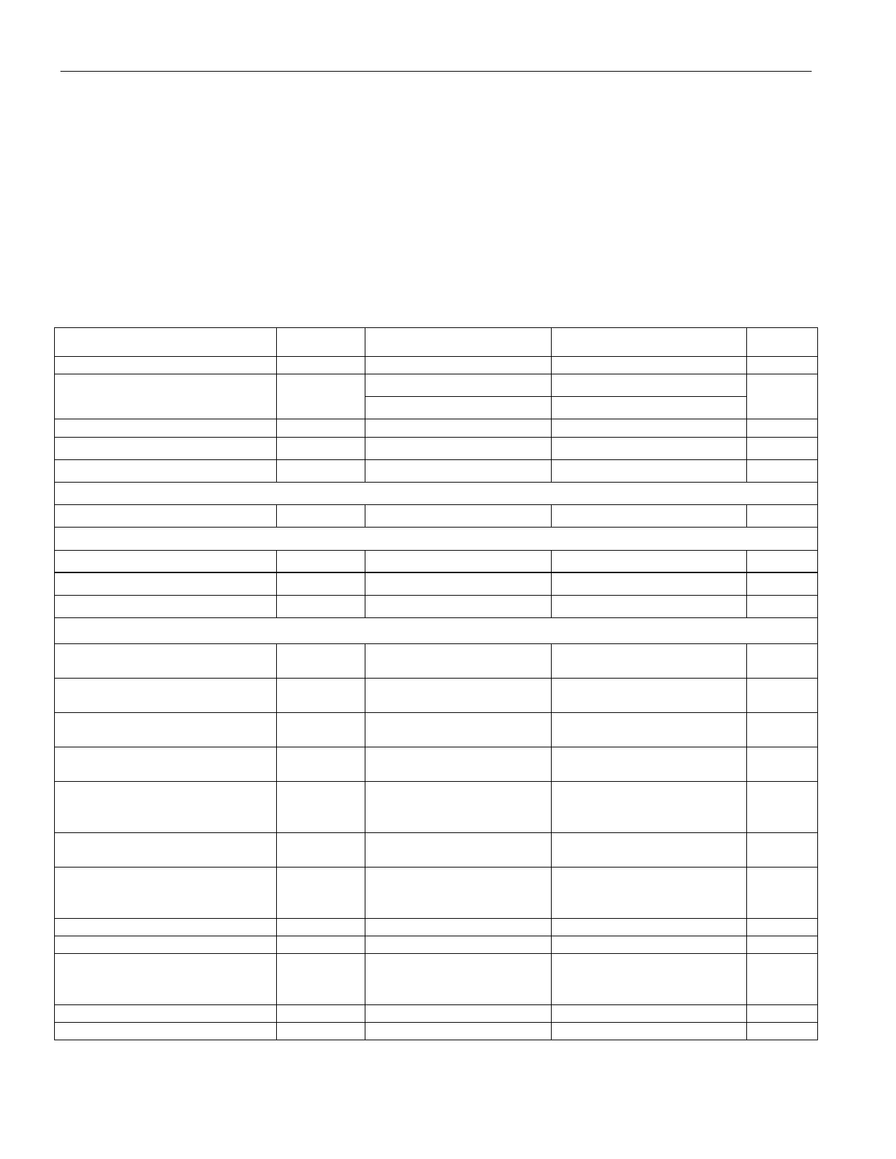
ELECTRICAL CHARACTERISTICS
PARAMETER
Supply Voltage
Standby Current
Operating Current
Programming Current
SHA-1 Computation Current
SHA-1 Engine
SHA-1 Computation Time
EEPROM
Programming Time
Endurance
Data Retention
I²C-Pins (Note 7) See Figure 6
SYMBOL
VCC
ICCS
ICCA
IPROG
ISHA
tSHA
tPROG
NCYCLE
tRET
CONDITIONS
Bus idle
Bus idle, +25°C
Bus active at 400kHz
See full version of data sheet
See full version of data sheet
At +25°C (Notes 2, 3)
At +85°C (Notes 4, 5, 6)
LOW Level Input Voltage
VIL
(Note 8)
HIGH Level Input Voltage
Hysteresis of Schmitt Trigger
Inputs
LOW Level Output Voltage at
4mA Sink Current
Output Fall Time from VIhmin to
VILmax with a Bus Capacitance
from 10pF to 400pF
Pulse Width of Spikes that are
Suppressed by the Input Filter
Input Current Each I/O Pin with
an Input Voltage Between
0.1VCCmax and 0.9VCCmax
Input Capacitance
SCL Clock Frequency
Hold Time (Repeated) START
Condition. After this Period, the
First Clock Pulse is Generated.
LOW Period of the SCL Clock
HIGH Period of the SCL Clock
VIH
Vhys
VOL
tof
tSP
Ii
Ci
fSCL
tHD:STA
tLOW
tHIGH
(Notes 8, 9)
(Note 9)
(Note 9)
SDA and SCL pins only
(Note 9)
(Notes 8, 10)
(Notes 8, 9)
MIN
2.7
200k
40
-0.5
0.7 ×
VCC
0.05 ×
VCC
20 +
0.1Cb
-10
0
0.6
1.3
0.6
(-40°C to +85°C, see Note 1)
TYP MAX UNITS
5.5
V
3
µA
1
250
500
µA
500
1000
µA
mA
ms
10
ms
years
0.3 ×
VCC
V
VCC +
0.5V
V
V
0.4
V
250
ns
50
ns
10
µA
10
pF
400
kHz
µs
µs
µs
2 of 8
Share Link: 