DS2460ST Просмотр технического описания (PDF) - Dallas Semiconductor -> Maxim Integrated
Номер в каталоге
Компоненты Описание
производитель
DS2460ST Datasheet PDF : 8 Pages
| |||
Abridged Data Sheet
DS2460
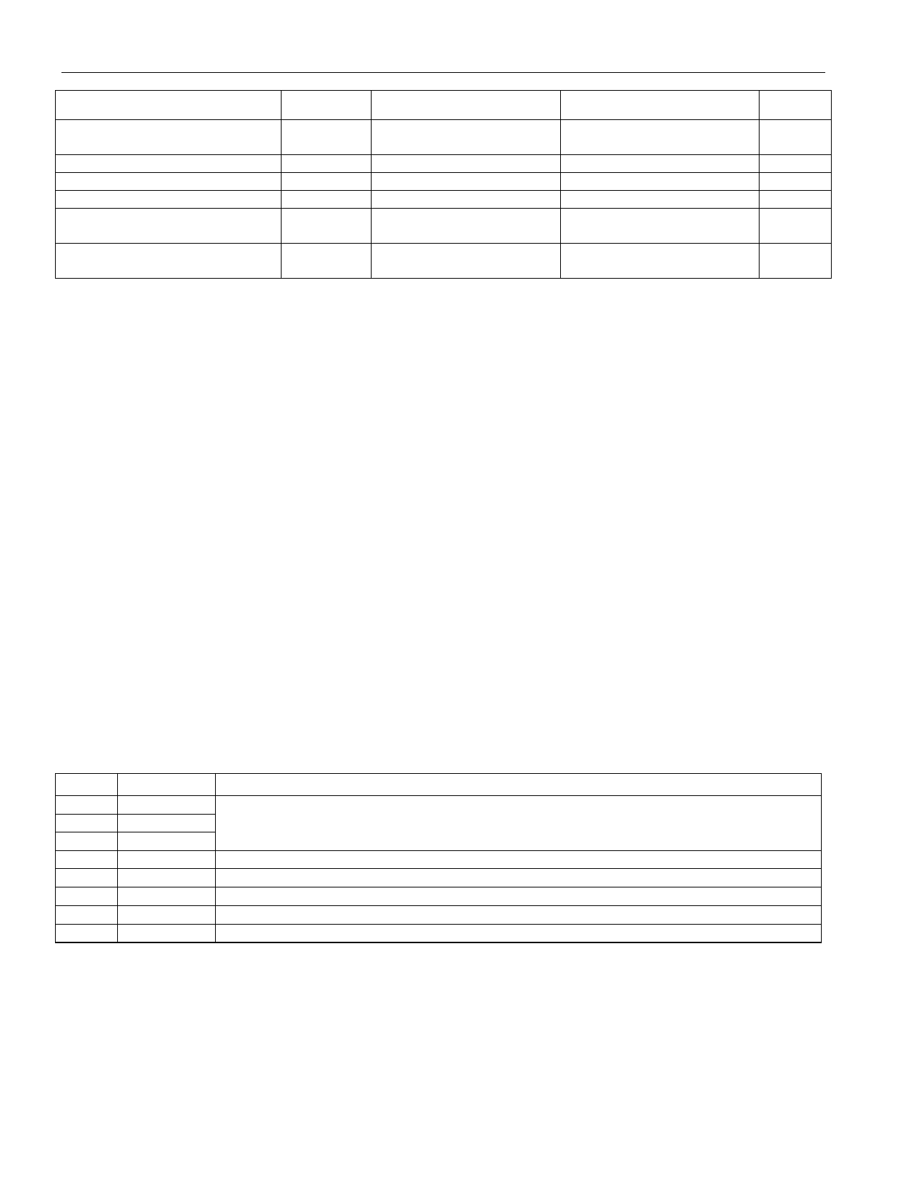
PARAMETER
Setup Time for a Repeated
START Condition
Data Hold Time
Data Setup Time
Setup Time for STOP Condition
Bus Free Time Between a
STOP and START Condition
Capacitive Load for Each Bus
Line
SYMBOL
tSU:STA
tHD:DAT
tSU:DAT
tSU:STO
tBUF
CB
CONDITIONS
(Notes 11, 12)
(Note 13)
(Note 14)
MIN TYP MAX UNITS
0.6
µs
0.9
µs
100
ns
0.6
µs
1.3
µs
400
pF
Note 1:
Note 2:
Note 3:
Note 4:
Note 5:
Note 6:
Note 7:
Note 8:
Note 9:
Note 10:
Note 11:
Note 12:
Note 13:
Note 14:
Specification at -40°C is guaranteed by design and characterization only and not production tested.
Write-cycle endurance is degraded as TA increases.
Not 100% production-tested; guaranteed by reliability monitor sampling.
Data retention is degraded as TA increases.
Guaranteed by 100% production test at elevated temperature for a shorter amount of time;
equivalence of this production test to data sheet limit at operating temperature range is established by
reliability testing.
EEPROM writes can become nonfunctional after the data-retention time is exceeded. Long-term
storage at elevated temperatures is not recommended; the device can lose its write capability after 10
years at +125°C or 40 years at +85°C.
All values are referred to VIHmin and VILmax levels.
Applies to SDA, SCL, AD2, AD1, AD0.
Guaranteed by simulation only, not production tested.
I/O pins of the DS2460 do not obstruct the SDA and SCL lines if VCC is switched off.
The DS2460 provides a hold time of at least 300ns for the SDA signal (referred to the VIHmin of the SCL
signal) to bridge the undefined region of the falling edge of SCL.
The maximum tHD:DAT has only to be met if the device does not stretch the LOW period (tLOW) of the
SCL signal.
A Fast-mode I²C-bus device can be used in a standard-mode I²C-bus system, but the requirement
tSU:DAT ≥250ns must then be met. This is automatically the case if the device does not stretch the LOW
period of the SCL signal. If such a device does stretch the LOW period of the SCL signal, it must
output the next data bit to the SDA line tr max + tSU:DAT = 1000 + 250 = 1250ns (according to the
standard-mode I²C-bus specification) before the SCL line is released.
CB = total capacitance of one bus line in pF. If mixed with HS-mode devices, faster fall-times according
to I²C-Bus Specification v2.1 are allowed.
PIN DESCRIPTION
PIN
NAME
FUNCTION
1
2
3
AD0
AD1
AD2
I²C Address Inputs; must be tied to VCC or GND. These inputs determine the I²C slave
address of the device, see Figure 5.
4
GND
Ground Reference
5
NC
Not Connected
6
SDA
I²C Serial Data Input/Output; must be tied to VCC through a pullup resistor.
7
SCL
I²C Serial Clock Input; must be tied to VCC through a pullup resistor.
8
VCC
Power Supply Input
OVERVIEW
The block diagram in Figure 1 shows the relationships between the major control and memory sections of the
DS2460. The DS2460 communicates with a host processor through its I²C bus interface in standard-mode or in
fast-mode. The logic state of three address pins determines the I²C slave address of the DS2460, allowing up to 8
devices to operate on the same bus segment without requiring a hub. For more information (including Figure 2)
refer to the full version of the data sheet.
3 of 8
Share Link: 